Passive Components Blog
No Result
View All Result
  • Home
  • NewsFilter
    • All
    • Aerospace & Defence
    • Antenna
    • Applications
    • Automotive
    • Capacitors
    • Circuit Protection Devices
    • electro-mechanical news
    • Filters
    • Fuses
    • Inductors
    • Industrial
    • Integrated Passives
    • inter-connect news
    • Market & Supply Chain
    • Market Insights
    • Medical
    • Modelling and Simulation
    • New Materials & Supply
    • New Technologies
    • Non-linear Passives
    • Oscillators
    • Passive Sensors News
    • Resistors
    • RF & Microwave
    • Telecommunication
    • Weekly Digest

    Inductor Resonances and its Impact to EMI

    Developing Low Inductance Film Capacitor using Bode 100 Analyzer

    Highly Reliable Flex Rigid PCBs, Würth Elektronik Webinar

    Würth Elektronik Releases High Performance TLVR Coupled Inductors

    YAGEO Extends Rectangular Aluminum Electrolytic Capacitor Family

    Dr. Tomas Zednicek Vision for Europe 2025 Passive Electronics Market

    Littelfuse Releases Industry-First SMD Fuse with 1500A Interrupting Rating at 277V

    TDK Unveils Industry Highest Rated Current Multilayer Chip Beads

    Vishay Releases Automotive SMD Thick Film Power Resistor for Enhanced Protection Against Short Transient Pulses

    Trending Tags

    • Ripple Current
    • RF
    • Leakage Current
    • Tantalum vs Ceramic
    • Snubber
    • Low ESR
    • Feedthrough
    • Derating
    • Dielectric Constant
    • New Products
    • Market Reports
  • VideoFilter
    • All
    • Antenna videos
    • Capacitor videos
    • Circuit Protection Video
    • Filter videos
    • Fuse videos
    • Inductor videos
    • Inter-Connect Video
    • Non-linear passives videos
    • Oscillator videos
    • Passive sensors videos
    • Resistor videos

    Inductor Resonances and its Impact to EMI

    Highly Reliable Flex Rigid PCBs, Würth Elektronik Webinar

    Causes of Oscillations in Flyback Converters

    How to design a 60W Flyback Transformer

    Modeling and Simulation of Leakage Inductance

    Power Inductor Considerations for AI High Power Computing – Vishay Video

    Coupled Inductors in Multiphase Boost Converters

    VPG Demonstrates Precision Resistor in Cryogenic Conditions

    Comparison Testing of Chip Resistor Technologies Under High Vibration

    Trending Tags

    • Capacitors explained
    • Inductors explained
    • Resistors explained
    • Filters explained
    • Application Video Guidelines
    • EMC
    • New Products
    • Ripple Current
    • Simulation
    • Tantalum vs Ceramic
  • Knowledge Blog
  • Suppliers
    • Who is Who
  • Events
No Result
View All Result
Passive Components Blog
No Result
View All Result

Platform Structure Clock Oscillators

19.1.2023
Reading Time: 9 mins read
A A

This blog article written by Toshihiko Koyanagi, published by KYOCERA-AVX Corporation describes platform structure clock oscillators and its features.

Introduction

Numerous devices in people‘s lives today are becoming more sophisticated. As a result, the number of crystal devices installed is increasing. For example, with the evolution of autonomous driving, we are using crystal devices for many functions such as sensor systems to detect distance, camera systems to capture images, image processing systems to process captured images, and communication systems to communicate many of those digital data in and out of the vehicle at high speed.

RelatedPosts

KYOCERA AVX Releases Compact High-Directivity Couplers

Kyocera Introducing SAW Filters for Implantable Medical and AED Applications

The Path to Thinner MLCCs and Innovative Capacitor Development

In addition, in the network market, the number of crystal devices is increasing along with the further increase in the speed of communication devices, as well as the increase in the frequency and precision.

Crystal Oscillator with Platform Structure

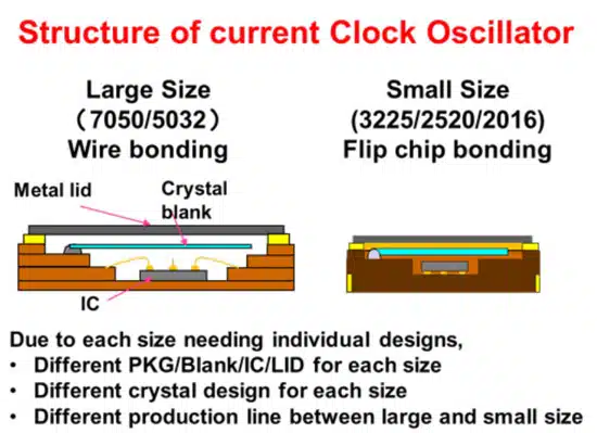
This section describes unique platform structure for clock oscillators. First, Figure 1 shows the structure of a conventional, typical clock oscillator, with examples of the large size 7050 and 5032 on the left and the small size 2016 ~ 3225 on the right.

In general, for each product size, the main component (Ceramic Package, Crystal Blank, IC, LID) must be prepared, and each size has a different design. For example, in the case of size 7050, we had to prepare different materials for each product size, such as a ceramic package of size 7050 and a quartz blank suitable for that size, or a package and blank of that size for a smaller size 2016. This has been one of the challenges of conventional oscillators.

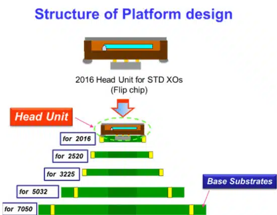
Figure 2 is KYOCERA AVX‘s unique platform structure. The platform structure consists of a head unit which is a standard 2016 size Crystal Unit using 2016 size ceramic package, crystal blank, IC and LID as the main components that control product characteristics. By mounting this head unit on a 2016 ~ 7050 size glass epoxy board, the physical size of the component itself is adjusted. Compared with conventional products, this structure enables major components of all sizes to be consolidated into a single size, making it possible to use common materials, resulting in shorter lead times.

Figure 1. Structure and issues of conventional crystal oscillators
Figure 2. Platform crystal oscillator structure; source: KYOCERA AVX

The other benefit of Platform design is “contributing to design simplification,” because the same characteristics can be achieved in all sizes by using common head units, and when customers downsize, the characteristics remain the same, which can reduce customers‘ evaluation time. Also KYOCERA AVX’s large-size parts also use the common head unit enabling long-term support.

Crystal oscillator platform structure design benefits:

  • Simplified design
  • Long-term supply
  • Improved reliability
  • Improved quality

Crystal Oscillator Platform Structure Reliability

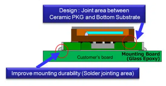
The platform structure may contribute to the improvement in junction reliability as explained in Figure 3.

Figure 3 shows platform structure Oscillator mounted on the customer’s PCB board with highlighted areas showing the junctions between the component and the board (left)/ bottom substrate (right).

Figure 3. Platform crystal oscillator structure with junctions highlights; source: KYOCERA AVX
Figure 4. Example of stress applied to solder after mounting (cold shock)
Figure 5. Ceramic Package solder joint crack example

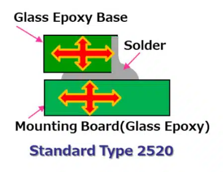
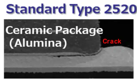
In the case of a cold shock, such as a TCT test, the conventional product structure requires direct solder-joining of the ceramic package, so the thermal expansion coefficient of the ceramic and customer’s PCB is different. Thus, residual stress remains on the solder joint which may result in cracks on the solder joint. (Figure 4). This may lead to solder joint crack as shown in Figure 5.

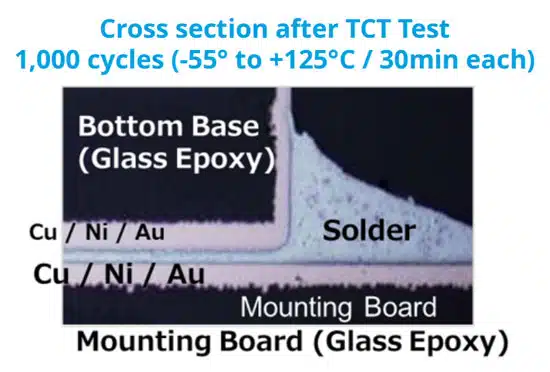
In the case of the platform structure, no stress is applied to the solder joint because the thermal expansion coefficient of customer’s board and KYOCERA AVX oscillator glass epoxy substrate are the same.

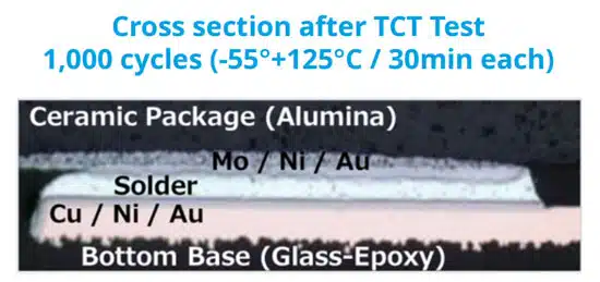
As Figure 6 shows, we confirmed there were no cracks in the joint even at 1,000 cycles at -55° ~125° C.

The junction of KYOCERA AVX ceramic package and glass epoxy board is also shown in Figure 3 – highlighted area on right. The ceramic package and glass epoxy substrate are electrically and mechanically connected by solder. In addition to that, the components are filled with epoxy resin between the ceramic package and the substrate. This design increases the strength of the joints.

Figure 7 shows a cross section of the relevant area. We can confirm that there are no cracks on the solder joints inside our product. The KYOCERA AVX platform structure is a structure with excellent junction reliability, and this is one of the features of this product.

Figure 6. Platform oscillator design solder junction cross section after 1000 temperature shock cycles
Figure 7. Platform oscillator design ceramic package and epoxy junction cross section after 1000 temperature shock cycles

Process Flow

The Figure 8. shows comparison of the conventional crystal oscillator process flow vs. platform structure oscillator design.

Figure 8. Conventional vs platform crystal oscillator process flow

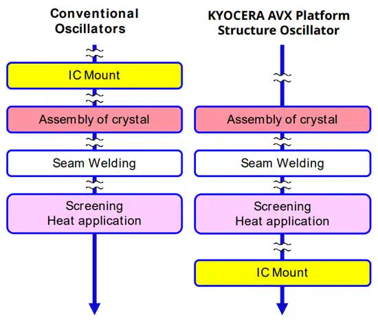
On the left is the process flow of a conventional type Oscillator. From its structural design, the IC is mounted on a ceramic package, on which a crystal blank is mounted, and the lid is welded. The problem with this conventional process flow is that the heat exceeding the heat-resistant temperature of the IC can not be applied to the crystal because the IC must be mounted before the crystal can be mounted.

Figure 9. Platform Z series crystal clock oscillator 2.5 x 2.0 mm Size

On the other hand, on the right hand side shows the process flow of platform structure, which shows the IC mounting process is after mounting the head unit. With no IC, it is now possible to apply high temperature heat that could not be applied with the IC mounted like the conventional type. The realization of this high-temperature heat treatment has made it possible to make defects in the crystal more obvious. This higher temperature heat treatment can also improve the reliability of aging.

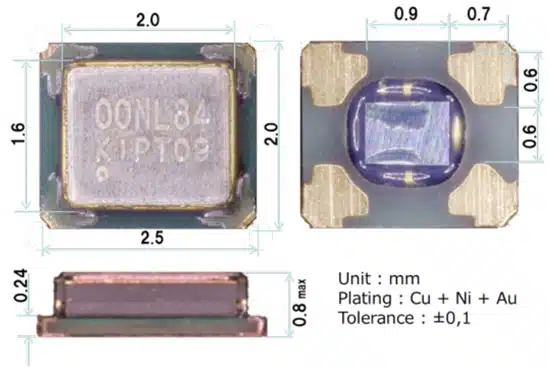
Figure 9 shows the physical photo of platform crystal oscillator. This is a 2.5mm x 2.0mm size Oscillator. The PIN layout is the same as the conventional type and can be mounted on the same land pattern as the current one.

Key Benefits of Platform Crystal Oscillator Design – Temperature Stability and Short Leadtime

Figure 10. High temperature and short leadtime benefits of platform crystal oscillator structure; source: KYOCERA AVX

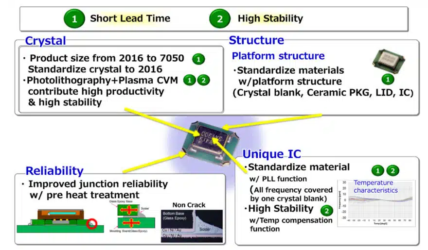
In Figure 10, the Z series’ platform crystal oscillator features are explained, which are short delivery time, high precision and stable supply. By following the platform structure, it is possible to consolidate all the crystal blanks that are used for sizes 2016 ~ 7050 into a single 2016 size. Also, the crystal blank used in this Z series is: KYOCERA AVX’s proprietary “Plasma CVM Method” is used for photolithography, a microfabrication technology, to achieve high productivity and high precision.

By adhering to the platform structure, the main components, such as crystal blanks, ceramic packages, LIDs, and ICs, which are the characteristics of the platform, do not differ according to the product size, making it possible to consolidate the components.

Reliability is also based on the platform structure, which improves junction reliability. Then there‘s IC (Unique IC). The ICs used in the Z series are KYOCERA AVX’s own custom ICs. One of the challenges with conventional IC products is the need to prepare a crystal blank for each frequency.

Figure 11 is a comparison of product features. We compared general structure Oscillators versus Platform Z-series. The tables show the presence or absence of a built-in PLL circuit, the presence or absence of a built-in temperature compensation circuit, the commonality of components, the frequency range supported, and the status of mass production support.

Figure 11. Comparison of conventional and platform structure oscillator features; source: KYOCERA AVX

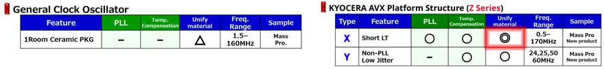
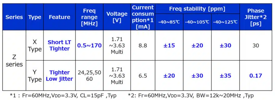
The X-Type in the Z Series is the most common type of product. If a high-precision response is required, the “Y Type” of the “Z Series” using the “Temperature Compensation Circuit“ can be the best fit. This custom IC has a built-in PLL function, which enables one frequency blank to handle all frequencies from 0.5 MHz to 170 MHz, and further consolidates the components. Another feature is the built-in temperature compensation circuit. By incorporating a temperature compensation circuit, it is possible to provide high-precision support, which is not possible with conventional products.

Figure 12 is a comparison of electrical characteristics. The table shows the electrical characteristics of “frequency range,” “power supply voltage,” “current consumption,” “frequency stability,” and “Jitter.” The content shown in blue is the characteristic part. The “X Type” of the “Z Series” is a standard product that uses a PLL and a temperature compensation circuit and is characterized by short delivery and high precision. The Y-type in the Z Series features high precision and low-phase noise using a temperature compensation circuit.

Figure 12. Comparison between X and Y type Z series platform crystal oscillators; source: KYOCERA AVX

Related

Source: KYOCERA AVX

Recent Posts

Inductor Resonances and its Impact to EMI

16.5.2025
10

Würth Elektronik Releases High Performance TLVR Coupled Inductors

15.5.2025
15

Causes of Oscillations in Flyback Converters

15.5.2025
9

How to design a 60W Flyback Transformer

12.5.2025
27

Murata Releases 008004 High-Frequency SMD Chip Inductor

12.5.2025
21

Modeling and Simulation of Leakage Inductance

9.5.2025
24

KYOCERA AVX Releases Compact High-Directivity Couplers

7.5.2025
24

Murata and NIMS Built New Database of Dielectric Material Properties

5.5.2025
59

Würth Elektronik Offers New Power Supplies Development Kit

29.4.2025
44

Shielding Cabinets

29.4.2025
27

Upcoming Events

May 28
16:00 - 17:00 CEST

Power Over Data Line

View Calendar

Popular Posts

  • Boost Converter Design and Calculation

    0 shares
    Share 0 Tweet 0
  • Buck Converter Design and Calculation

    0 shares
    Share 0 Tweet 0
  • Flyback Converter Design and Calculation

    0 shares
    Share 0 Tweet 0
  • LLC Resonant Converter Design and Calculation

    0 shares
    Share 0 Tweet 0
  • What is a Dielectric Constant and DF of Plastic Materials?

    4 shares
    Share 4 Tweet 0
  • SEPIC Converter Design and Calculation

    0 shares
    Share 0 Tweet 0
  • Why Low ESR Matters in Capacitor Design

    0 shares
    Share 0 Tweet 0
  • What is the Difference Between X8G, X8L and X8R Ceramic Capacitor Dielectrics?

    0 shares
    Share 0 Tweet 0
  • Ripple Current and its Effects on the Performance of Capacitors

    3 shares
    Share 3 Tweet 0
  • Inductor Resonances and its Impact to EMI

    0 shares
    Share 0 Tweet 0

Newsletter Subscription


Passive Components Blog

© EPCI - Leading Passive Components Educational and Information Site

  • Home
  • Privacy Policy
  • EPCI Membership & Advertisement
  • About

No Result
View All Result
  • Home
  • Knowledge Blog
  • Premium Suppliers

© EPCI - Leading Passive Components Educational and Information Site

This website uses cookies. By continuing to use this website you are giving consent to cookies being used. Visit our Privacy and Cookie Policy.
Go to mobile version