Passive Components Blog
No Result
View All Result
  • Home
  • NewsFilter
    • All
    • Aerospace & Defence
    • Antenna
    • Applications
    • Automotive
    • Capacitors
    • Circuit Protection Devices
    • electro-mechanical news
    • Filters
    • Fuses
    • Inductors
    • Industrial
    • Integrated Passives
    • inter-connect news
    • Market & Supply Chain
    • Market Insights
    • Medical
    • Modelling and Simulation
    • New Materials & Supply
    • New Technologies
    • Non-linear Passives
    • Oscillators
    • Passive Sensors News
    • Resistors
    • RF & Microwave
    • Telecommunication
    • Weekly Digest

    Bourns Releases Automotive 1W Flyback Transformer

    Wk 20 Electronics Supply Chain Digest

    Inductor Resonances and its Impact to EMI

    Developing Low Inductance Film Capacitor using Bode 100 Analyzer

    Highly Reliable Flex Rigid PCBs, Würth Elektronik Webinar

    Würth Elektronik Releases High Performance TLVR Coupled Inductors

    YAGEO Extends Rectangular Aluminum Electrolytic Capacitor Family

    Dr. Tomas Zednicek Vision for Europe 2025 Passive Electronics Market

    Littelfuse Releases Industry-First SMD Fuse with 1500A Interrupting Rating at 277V

    Trending Tags

    • Ripple Current
    • RF
    • Leakage Current
    • Tantalum vs Ceramic
    • Snubber
    • Low ESR
    • Feedthrough
    • Derating
    • Dielectric Constant
    • New Products
    • Market Reports
  • VideoFilter
    • All
    • Antenna videos
    • Capacitor videos
    • Circuit Protection Video
    • Filter videos
    • Fuse videos
    • Inductor videos
    • Inter-Connect Video
    • Non-linear passives videos
    • Oscillator videos
    • Passive sensors videos
    • Resistor videos

    Inductor Resonances and its Impact to EMI

    Highly Reliable Flex Rigid PCBs, Würth Elektronik Webinar

    Causes of Oscillations in Flyback Converters

    How to design a 60W Flyback Transformer

    Modeling and Simulation of Leakage Inductance

    Power Inductor Considerations for AI High Power Computing – Vishay Video

    Coupled Inductors in Multiphase Boost Converters

    VPG Demonstrates Precision Resistor in Cryogenic Conditions

    Comparison Testing of Chip Resistor Technologies Under High Vibration

    Trending Tags

    • Capacitors explained
    • Inductors explained
    • Resistors explained
    • Filters explained
    • Application Video Guidelines
    • EMC
    • New Products
    • Ripple Current
    • Simulation
    • Tantalum vs Ceramic
  • Knowledge Blog
  • Suppliers
    • Who is Who
  • Events
No Result
View All Result
Passive Components Blog
No Result
View All Result

Printed Circuit Boards

9.9.2021
Reading Time: 4 mins read
A A

Figure 2.64 schematically illustrates the components of a multilayer PCB prior to laminating. This PCB will have six layers.

Fig. 2.64: Multilayer Printed Circuit Board

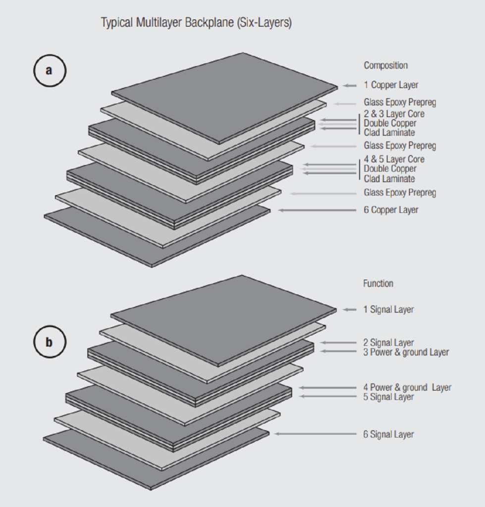
Each layer consists of an FR4, fiberglass epoxy substrate with copper circuitry on both sides of the substrate. The thickness and distribution of the copper depends on whether the function of the circuitry is to carry signal currents, milliamps to a few amps, or power, tens of amps. A bonding medium, prepreg, is placed between each pair of layers. In this example, starting from the top, the first layer has signal traces on each side. The second layer has a power/ground plane on each side. The third and fourth layers also have signal traces on each side. In the manufacturing process these four layers and the prepreeg are stacked and laminated under heat and pressure to create a multilayer PCB.

RelatedPosts

Polymer Materials and Processing

What is RF Connector

Connector Materials and Processes

Fig. 2.65: Multilayer PCB cross section

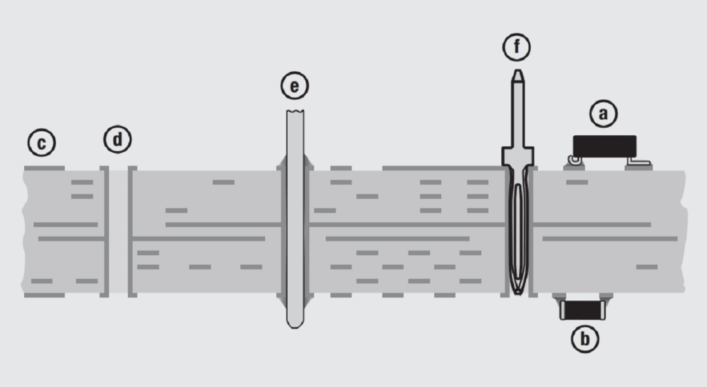
Figure 2.65 illustrates a cross section of the laminated PCB described. The small rectangles shown in the first, third and fourth layers are signal traces that run between the many devices that are mounted on the PCB. The power and ground planes in the second layer are continuous with the exception of holes in the planes to allow inter-connections to be made between the first, third and fourth layer circuitry using Plated Through Holes, PTH, three of which are shown in the drawing.

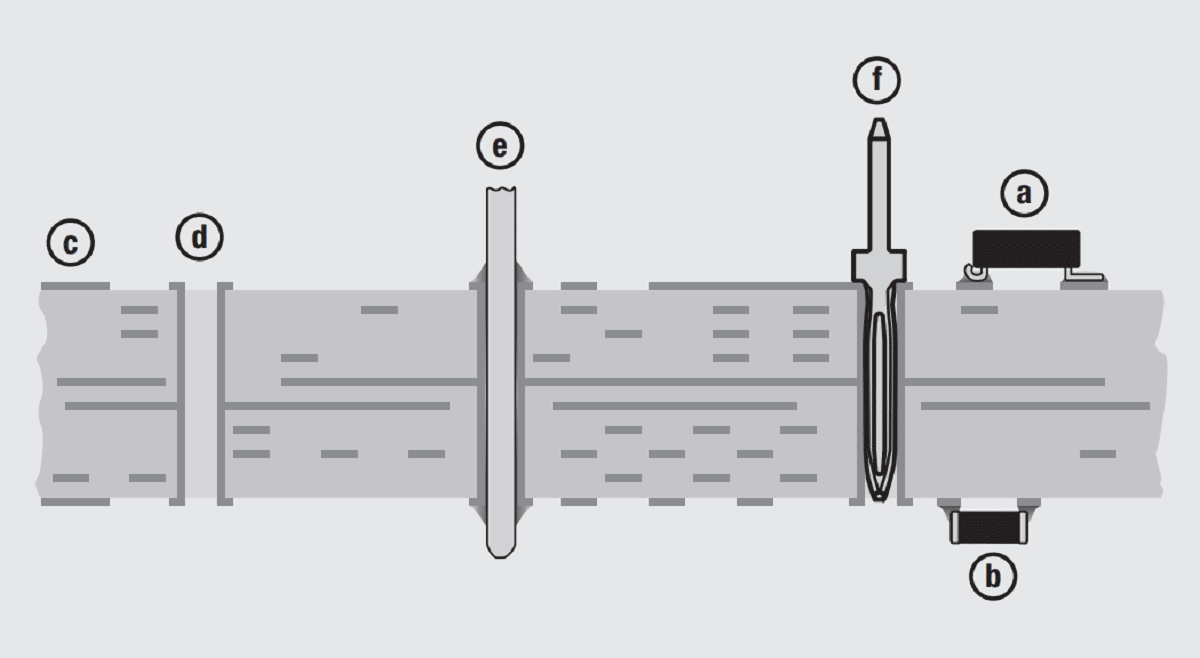
Consider now the variety of connections, mechanical and soldered, that can be made to this PCB. Note that some of the signal traces are on the surfaces of the PCB. Expanded areas along a surface trace to allow contacts to be made to the trace are called lands or pads. In addition to the copper circuitry, lands require an additional plating with the plating composition and thickness depending on the intended use of the pad, in particular whether mechanical or soldered connections will be made to the land. The plating considerations will be discussed with each application.

The top right component, Figure 2.66a, is soldered to surface pads on the PCB. For convenience, two different lead geometries, J-lead and Gull Wing are shown. In practice, of course, a component will use a single lead style. These geometries are two of the more commonly used methods for providing lead compliance to the soldered connection to minimize the effects of differential thermal expansion stresses on the solder joint as will be discussed in the section on SMT. Similar geometries are used as leads on connectors intended for SMT applications for the same reason. The PCB pads that are to be soldered will generally be treated so as to maintain or provide solderability of the base copper circuitry. Clean copper is readily solderable, but given the tendency of copper to corrode, the copper surface may receive an organic coating or a thin gold plating to prevent such corrosion and maintain the copper solderability. A second approach is to plate the copper with a solderable coating, tin depending on the environmental requirements to be met. The tin coating is generally screened on to the copper and reflowed. The coating thickness is typically of the order of 2 to 4 µm.

The bottom right component, Figure 2.65b, is a flip chip package which is soldered to the surface pads of the PCB using solder bumps or columns, a design sometimes called a leadless package. The plating requirement for this application is essentially the same as discussed for the previous component.

The pads on the left edge of the board, Figure 2.65c, are intended to mate to a card edge connector. The plating on the pad must be compatible with that on the card edge connector which is either gold over nickel or tin. The plating thicknesses on card-edge pads are typically in the range of 0.4–0.8 µm (15 to 30 microinches) for the gold and 1.25 to 2.5 µm (50 to 100 microinches) for the nickel. For tin coatings the thickness will be of the order of 2.5 µm (100 microinches). In addition to card edge connections, Central Processor Units, CPU are also connected to surface lands on multilayer boards. A Land Grid Array, LGA, socket contains spring contacts which are sandwiched between the lands on the PCB and the associated pads on the CPU package. LGA sockets use gold over nickel platings with the thicknesses noted above.

The three PTH connections are all different. As illustrated, Figure 2.65d shows a PTH that is used to make connections between layers within the board. For such applications a copper plating is generally used, the thickness depending on the current requirements to be supported. In this example the press-in solder contact, Figure 2.65e, makes a connection to one of the power/ground planes. A press-in solder pin is generally a solid, rigid pin and exerts only enough force to hold the pin in place until it is soldered, generally wave soldered. In contrast, the compliant press-in pin, Figure 2.65f, is intended to provide a robust mechanical permanent connection without the need for solder.

Two different permanent connection technologies, compliant press-in pins and soldering, have been introduced in this introductory section. Each will now be discussed individually.

Related

Source: Wurth elektronik

Recent Posts

Non-Magnetic Interconnects

23.4.2025
14

10 Tips for Ensuring Reliability of Discrete Wire Assemblies

20.2.2025
50

Polymer Materials and Processing

31.1.2025
35

Basic PCB Technology Overview

17.12.2024
15

What is RF Connector

17.12.2024
7

Creepage and Clearance of Connector

16.10.2023
12

Microwave Multi Line Connectors Mounting and Handling Precautions

17.12.2024
2

BASIC PCB Design Rules – Layout

17.12.2024
21

MEMR RF Relay for Space Compact Redundancy Ring

17.12.2024
2

Connector Temperature Rise and Derating

13.1.2023
12

Upcoming Events

May 28
16:00 - 17:00 CEST

Power Over Data Line

View Calendar

Popular Posts

  • Buck Converter Design and Calculation

    0 shares
    Share 0 Tweet 0
  • Flyback Converter Design and Calculation

    0 shares
    Share 0 Tweet 0
  • Boost Converter Design and Calculation

    0 shares
    Share 0 Tweet 0
  • LLC Resonant Converter Design and Calculation

    0 shares
    Share 0 Tweet 0
  • Why Low ESR Matters in Capacitor Design

    0 shares
    Share 0 Tweet 0
  • SEPIC Converter Design and Calculation

    0 shares
    Share 0 Tweet 0
  • What is a Dielectric Constant and DF of Plastic Materials?

    4 shares
    Share 4 Tweet 0
  • Ripple Current and its Effects on the Performance of Capacitors

    3 shares
    Share 3 Tweet 0
  • Flying Capacitors Explained

    0 shares
    Share 0 Tweet 0
  • NVIDIA GB300 Boost Hybrid Supercapacitor Demand

    0 shares
    Share 0 Tweet 0

Newsletter Subscription


Passive Components Blog

© EPCI - Leading Passive Components Educational and Information Site

  • Home
  • Privacy Policy
  • EPCI Membership & Advertisement
  • About

No Result
View All Result
  • Home
  • Knowledge Blog
  • Premium Suppliers

© EPCI - Leading Passive Components Educational and Information Site

This website uses cookies. By continuing to use this website you are giving consent to cookies being used. Visit our Privacy and Cookie Policy.
Go to mobile version