








Passive Components Blog
No Result
View All Result
  • Home
  • News
    • All
    • Aerospace & Defence
    • Antenna
    • Applications
    • Automotive
    • Capacitors
    • Circuit Protection Devices
    • electro-mechanical news
    • Filters
    • Fuses
    • Inductors
    • Industrial
    • Integrated Passives
    • inter-connect news
    • Market & Supply Chain
    • Market Insights
    • Medical
    • Modelling and Simulation
    • New Materials & Supply
    • New Technologies
    • Non-linear Passives
    • Optoelectronics and Isolation
    • Oscillators
    • Passive Sensors News
    • Resistors
    • RF & Microwave
    • Telecommunication
    • Weekly Digest
    Würth Elektronik WE-LHMI and WE-HCI power inductor comparison slide showing current ratings and maximum operating temperatures

    Power Inductor Selection: Ferrite vs Powder Core Trade-Offs, Würth Elektronik Webinar

    Bourns PWR163 DPAK-style surface-mount power resistor with moulded housing, metal backplate and terminals

    Bourns Releases Power Resistor Adds Reverse-Pin Configuration

    Conceptual polypropylene DC-link film capacitor module with parallel cells and copper interconnections

    DC-Link Film Capacitor Modules: Inductance and Thermal Design, Jianghai-Europe Tech Memo

    Panasonic EVP-BX surface-mount tactile switches with top-push actuators and two-terminal construction

    Panasonic EVP-BX Quiet Tactile Switches for HMI Designs

    Motor Run Capacitor Safety Classes S0–S3: A Design Guide

    YAGEO Piezoelectric Sensors for Predictive Maintenance

    Wk 44 Electronics Supply Chain Digest

    TDK HVC28 and HVC29 high-voltage DC contactors with black housings and main power terminals

    TDK Introduces Gas-Filled High-Voltage DC Contactors up to 600 A

    Murata SWL RF coaxial switch connector measurement diagram and SWL-to-SWJ board-area comparison.

    Murata RF Switch Connectors Cut PCB Test-Point Area

    Trending Tags

    • Ripple Current
    • RF
    • Leakage Current
    • Tantalum vs Ceramic
    • Snubber
    • Low ESR
    • Feedthrough
    • Derating
    • Dielectric Constant
    • New Products
    • Market Reports
  • Knowledge Blog
  • Dossiers
    • Aerospace and Defense Passive Components Dossier
    • AI Hardware Dossier
    • Automotive Dossier
    • Industrial Robotics Dossier
    • Power Converter Dossier
    • Capacitor Dossier
    • Circuit Protection Dossier
    • Inductor Dossier
    • Resistor Dossier
    • Silicon Capacitors and Integrated Passives Dossier
  • Suppliers
    • Who is Who
  • PCNS
    • PCNS 2025
    • PCNS 2023
    • PCNS 2021
    • PCNS 2019
    • PCNS 2017
  • Events
  • Home
  • News
    • All
    • Aerospace & Defence
    • Antenna
    • Applications
    • Automotive
    • Capacitors
    • Circuit Protection Devices
    • electro-mechanical news
    • Filters
    • Fuses
    • Inductors
    • Industrial
    • Integrated Passives
    • inter-connect news
    • Market & Supply Chain
    • Market Insights
    • Medical
    • Modelling and Simulation
    • New Materials & Supply
    • New Technologies
    • Non-linear Passives
    • Optoelectronics and Isolation
    • Oscillators
    • Passive Sensors News
    • Resistors
    • RF & Microwave
    • Telecommunication
    • Weekly Digest
    Würth Elektronik WE-LHMI and WE-HCI power inductor comparison slide showing current ratings and maximum operating temperatures

    Power Inductor Selection: Ferrite vs Powder Core Trade-Offs, Würth Elektronik Webinar

    Bourns PWR163 DPAK-style surface-mount power resistor with moulded housing, metal backplate and terminals

    Bourns Releases Power Resistor Adds Reverse-Pin Configuration

    Conceptual polypropylene DC-link film capacitor module with parallel cells and copper interconnections

    DC-Link Film Capacitor Modules: Inductance and Thermal Design, Jianghai-Europe Tech Memo

    Panasonic EVP-BX surface-mount tactile switches with top-push actuators and two-terminal construction

    Panasonic EVP-BX Quiet Tactile Switches for HMI Designs

    Motor Run Capacitor Safety Classes S0–S3: A Design Guide

    YAGEO Piezoelectric Sensors for Predictive Maintenance

    Wk 44 Electronics Supply Chain Digest

    TDK HVC28 and HVC29 high-voltage DC contactors with black housings and main power terminals

    TDK Introduces Gas-Filled High-Voltage DC Contactors up to 600 A

    Murata SWL RF coaxial switch connector measurement diagram and SWL-to-SWJ board-area comparison.

    Murata RF Switch Connectors Cut PCB Test-Point Area

    Trending Tags

    • Ripple Current
    • RF
    • Leakage Current
    • Tantalum vs Ceramic
    • Snubber
    • Low ESR
    • Feedthrough
    • Derating
    • Dielectric Constant
    • New Products
    • Market Reports
  • Knowledge Blog
  • Dossiers
    • Aerospace and Defense Passive Components Dossier
    • AI Hardware Dossier
    • Automotive Dossier
    • Industrial Robotics Dossier
    • Power Converter Dossier
    • Capacitor Dossier
    • Circuit Protection Dossier
    • Inductor Dossier
    • Resistor Dossier
    • Silicon Capacitors and Integrated Passives Dossier
  • Suppliers
    • Who is Who
  • PCNS
    • PCNS 2025
    • PCNS 2023
    • PCNS 2021
    • PCNS 2019
    • PCNS 2017
  • Events
No Result
View All Result
Passive Components Blog
No Result
View All Result

Researches Developed New Technology for 3D Print of High Conductivity Metal Materials

21.4.2020
Reading Time: 6 mins read
A A

New technique boosts versatility of 3D-printed metals. Electrical engineering research team of Arizona State University devises method to improve conductivity and performance of metallic materials.

Advances in the capabilities of 3D printing technology have been achieved at a steady pace in recent years. But most of the progress has involved the printing of relatively pliable materials. Potential solutions for each of those problems may spring from results of recent research led by Chao Wang and Yu Yao, assistant professors of electrical, computer and energy engineering in the Ira A. Fulton Schools of Engineering at Arizona State University.

RelatedPosts

Power Inductor Selection: Ferrite vs Powder Core Trade-Offs, Würth Elektronik Webinar

Bourns Releases Power Resistor Adds Reverse-Pin Configuration

DC-Link Film Capacitor Modules: Inductance and Thermal Design, Jianghai-Europe Tech Memo

Wang and Yao’s teams have developed a novel additive manufacturing technique that, unlike existing techniques, can print continuous and smooth films with high electrical and optical performance while at room-temperature and at low costs — something never done before, Wang points out.

The 3D printing process is based on optical projection, similar to playing movies using a projector, to create programmed ultraviolet light illumination in a precursor solution, which is used to catalyze a chemical reaction. The UV light triggers photochemical reactions for metal nucleation and growth.

“Projectors play movies made of multiple frames of images. Slightly different from movie projectors, we need to use only a single color from the light, which is ultraviolet, to print a single image through the photochemical deposition,” Wang said. “The projected patterns in light intensity are faithfully replicated in the metal patterns, and displayed as a portrait of complex metallic structures.”

The same process is also excellent for printing high-quality metal structures made of noble metals such as gold, silver and platinum and has the added attractions of enabling low-cost manufacturing of a variety of metal materials. As a proof-of-concept demonstration, the team printed the ASU mascot “Sparky” and the ASU pitchfork and sunburst logos in platinum, gold, and silver together on a single piece of glass (see illustration below).
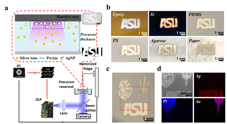
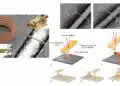
examples of the ASU logo printed on different materials
The illustration from “Printing continuous metal structures via polymer-assisted photochemical deposition” in the research journal Materials Today depicts key phases of a new method for 3D printing metals at the micrometer scale. The technique developed by a team of Fulton Schools electrical engineering researchers produced improved high-performance metals for a broad range of technological applications. As an example, the team printed metal on a variety of different materials, including glass, silicon, plastics, gel and paper. They also printed the ASU mascot “Sparky,” the ASU pitchfork and sunburst logos in platinum, gold and silver to prove the versatility of this technique. Illustration courtesy of Chao Wang/ASU

“In principle, we can engineer the optical properties of such metal to produce color images,” Wang said.

The process is versatile, he said, because it enables flexible designs of the printed patterns for broad range of applications in microelectronics, photonics, energy and health care.

An important advantage offered by the research team’s new additive manufacturing process is that it can be done at room temperature, Wang says. Current manufacturing processes use high temperatures, which significantly limit their capacity to print on materials that are susceptible to heat, particularly the kinds of materials typically used in flexible electronics, robotics and biosensors.

Breakthrough in preventing defects in 3D-printed material

In contrast to other 3D printing techniques, the research team added a small amount of polymer with many ligands (groups of chemicals) into a precursor solution at the start of 3D printing process. The ligands interact with synthesized particles to overcome their electrostatic repulsion, which is useful in stabilizing particles during synthesis but prevents them from connecting into a smooth film, Wang says.

At this point, the polymer acts as a chain that connects synthesized nanoparticles, and thus makes the final product a connected and continuous film rather than one riddled with small holes that separate the particles and cause considerable electrical and optical energy loss.

“In this way, we eliminate gaps between nanoparticles, something not done by other technologies,” Wang said. “The polymer acts as a super glue that tethers the nanoparticles together through the polymers’ chemical reactions with the metal particles.”

Importantly, he emphasizes, the method — using the technique described above and dubbed as polymer-assisted photochemical deposition — produces materials with high electrical conductivity and optical reflectivity.

New method opens door to upgrades in multiple technologies

With those characteristics, the team foresees the new 3D printing technology being especially useful for producing metallic contacts for various electronic, optoelectronic and biosensing devices, especially flexible devices with 3D configurations.

For microelectronics and flexible electronics, Wang says, the high conductivity of metal materials produced by the manufacturing method can provide a higher current at the supplied voltage. Therefore, less energy is lost on the metal interconnections and more energy can be allocated to critical parts of the devices, such as displays, memory and central processing units for computers, smartphones and tablets.

In solar energy applications, for instance, highly reflective metal films are needed to focus sunlight onto a collector that stores energy. The reflectivity of the metal film has a significant impact on the optical efficiency of the collection of sunlight, and thus on the system’s power output.

As another example of the applications, Yao points to optical devices, such as mirrors and filters that require highly reflective metal coatings. Thermal shields, for instance, that are widely used in aerospace applications, need thin film reflective foils that will provide thermal insulation for satellites and manned and unmanned spacecraft by reflecting the incoming radiation from the sun.

The series of graphic images demonstrates the range high-quality 3D printing of complex microstructures and 3D patterns enabled by the research of Fulton Schools electrical engineers, including printed microstructures for electronic circuits, a portrait of a toddler and two images of a 3D silver network printed on top of a hemisphere.

In addition, Yao emphasizes, the manufacturing technique can also enable making 3D microscale or even nanoscale optical structures on a large scale with low cost, which is highly desirable for implementation of ultra-compact, high-performance metamaterial and metasurface devices for a broad range of electromagnetic spectra ranging from visible light to radio frequencies.
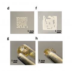
microscope designs with metal
The series of graphic images demonstrates the range high-quality 3D printing of complex microstructures and 3D patterns enabled by the research of Fulton Schools electrical engineers, including printed microstructures for electronic circuits, a portrait of a toddler and two images of a 3D silver network printed on top of a hemisphere. Courtesy of Chao Wang/ASU

“Similar to the movie-playing concept, the printing process can be repeated multiple times with a different image in each printing step, thus building up more complex structures, such as 3D structures on curved surfaces,” Yu said. “This could enable creating on-chip integrated 3D devices that are otherwise difficult to make, including 3D inductors for technologies using radio frequency capabilities.”

Along with the high quality of printing produced by polymer-assisted photochemical deposition technique, the researchers expect it to be useful in producing components and devices for soft robotics, responsive coatings, solar energy harvesting devices, energy storage technologies, intelligent electromagnetic devices, biochemical sensors and other smart biomedical devices.

Details are provided in the recent paper published in the research journal Materials Today.

Wang’s and Yao’s co-authors are Zhi Zhao and Jing Bai. Wang and Yao teach in the School of Electrical, Computer and Energy Engineering, one of the six Fulton Schools. Zhao was until recently a postdoctoral researcher working with both Wang’s and Yao’s research groups. Bai is an electrical engineering doctoral student who works with Yao. Bai was involved in the design, fabrication and characterization of printed metal films, which is important to understanding the electrical performance of the films.

The research was supported by the National Science Foundation, or NSF, and by startup funding provided to Wang and Yao by ASU. 

Based on their team’s results, the NSF is now supporting Wang and Yao on a project to develop higher-resolution silver-printing technology for applications in functional electronics and photonics

Related

Source: Arizona State University

Recent Posts

Features of BCZT and strontium titanate dielectric layers in a thin-film superlattice

Relaxor superlattice capacitors approach 99% efficiency

12.10.2026
47
tungsten-bronze-ceramic-capacitor-stack

Tungsten bronze capacitors combine high κ and thermal stability

7.10.2026
46
Schematic of the step-wise LPG/LPG@MnOx/LPG-O functionally graded thick cathode for a zinc-ion hybrid capacitor, Hefei Institutes of Physical Science.

Laser-Engineered Zinc-Ion Cathodes Target Thick Electrodes

1.10.2026
20
Antiferroelectric hafnia crystal structure showing alternating polar layers and field-aligned polar state, University of Nebraska–Lincoln

Antiferroelectric Hafnia at the 2D Limit

29.9.2026
37

On-Chip 3D-Printed Copper Microinductors: A New Route to Compact RF Electronics

10.9.2026
53
Overview of fabricated ferroelectric capacitors improving hyperdimensional computing task learning accuracy. a The experimental work reported in this study comprises ferroelectric capacitor (FeCAP) device fabrication, structural and electrical characterization, analog state identification and their reliability study. b The computational part of the work explores the benefits of using characteristics from the fabricated devices in a hyperdimensional computing scheme; source: authors

High-Precision Hyperdimensional Computing with Multi-Level Ferroelectric HZO Capacitors

7.9.2026
40

Ultrahigh Energy Storage in Lead‑Free BiFeO₃‑Based Ceramic Capacitors via Local Polar Structure Design

16.6.2026
82

Imec Presents High-density MIMCAP RF interposer for III-V chiplets

15.6.2026
167

All‑Water Supercapacitor Based on 1‑nm Clay Channels and Nanoconfined Water Electrolyte

10.6.2026
118

Upcoming Events

Nov 24
16:00 - 17:00 CET

Select the Correct Components for Your DC/DC Converter

Dec 1
16:00 - 17:00 CET

Developing low-noise mixed-signal systems

Dec 8
16:00 - 17:00 CET

WE-CCMF: Design Principles, Layout Guidelines and Measurement Results for High-Speed EMI Filtering

View Calendar

Popular Posts

  • Buck Converter Design and Calculation

    0 shares
    Share 0 Tweet 0
  • Boost Converter Design and Calculation

    0 shares
    Share 0 Tweet 0
  • September 2026 Interconnect, Passives and Electromechanical Components Market Insights

    0 shares
    Share 0 Tweet 0
  • LLC Resonant Converter Design and Calculation

    0 shares
    Share 0 Tweet 0
  • Capacitor Charging and Discharging

    0 shares
    Share 0 Tweet 0
  • Flyback Converter Design and Calculation

    0 shares
    Share 0 Tweet 0
  • RF Connector Types: How To Choose the Right One

    0 shares
    Share 0 Tweet 0
  • Passive Low Pass Filters: Fundamentals and EMI Design

    0 shares
    Share 0 Tweet 0
  • MLCC and Ceramic Capacitors

    0 shares
    Share 0 Tweet 0
  • Audio Capacitors: Choosing Capacitors for Crossover Circuits

    0 shares
    Share 0 Tweet 0

Newsletter Subscription


Passive Components Blog

© 2015–2026
All rights reserved

  • Home
  • Privacy Policy
  • EPCI Membership & Advertisement
  • About

No Result
View All Result
  • Home
  • Knowledge Blog
  • Dossiers
  • PCNS

© 2015–2026
All rights reserved