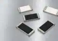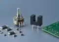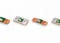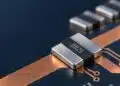







This guideline provides a structured way to select resistor technologies, benchmark their capabilities, and map them to concrete design use‑cases. It is intended as a practical design aid rather than a datasheet replacement.
This article focuses on choosing the appropriate resistor technology and package for a given circuit function. It is intended to complement, not replace, the dedicated articles on thin‑film, thick‑film, wirewound, MELF, and other resistor constructions available in the Passive Components Blog, where the physical principles and detailed design rules for each technology are covered in depth.
Key Takeaways
- Start resistor selection by checking hard limits: resistance range, power dissipation, voltage stress, pulse/surge profile, and required bandwidth. Technologies that cannot survive these stresses are excluded up front.
- Once survivability is assured, accuracy requirements (tolerance, TCR, matching, and long‑term drift) determine whether thick film, thin film, metal foil, or metal element shunts are appropriate.
- Environmental conditions and application class (commercial, industrial, automotive) strongly influence technology choice; AEC‑Q200‑qualified series are preferred for automotive and other harsh or safety‑relevant designs.
- Thick‑film chips cover most cost‑sensitive, general‑purpose uses, while thin‑film and foil resistors dominate precision analog, metrology, and high‑frequency matching; metal strip shunts and wirewound/metal oxide parts serve high‑current, high‑power, and surge‑critical positions.
- Layout, parasitic effects, and thermal management are often as important as the resistor body: Kelvin connections, low‑inductance geometries, and, for RF parts, use of S‑parameter‑based simulation are key to achieving the expected in‑circuit performance.
Follow this guide with recommendations How to choose the best resistor technology:
1. How to Choose a Resistor Technology – Step‑by‑Step
1.1 Step 1 – Define Electrical Stresses (R, P, V, Pulse, Frequency)
Start by bounding the operating stresses. Any technology that cannot survive them is excluded regardless of cost or precision.
Resistance value (R)
- Very low resistance
- Roughly ≤10 mΩ to a few 100 mΩ.
- Typical technologies: metal element (shunt), specialized low‑ohmic metal or thin film, some wirewound.
- Avoid standard thick film or carbon film here if you need accurate current sensing or stable calibration.
- Medium resistance
- Roughly 1 Ω to 1 MΩ.
- All mainstream technologies are available (thick film, thin/metal film, wirewound, carbon, metal oxide, foil).
- Selection is driven by accuracy, temperature coefficient, noise, and cost.
- High and very high resistance
- Roughly ≥10 MΩ up to 100 MΩ and beyond.
- Common technologies: thick film, metal glaze/metal oxide, some carbon film; thin film usually limited at the upper end of this range.
- Moisture and contamination effects become critical; derate both voltage and power.
Power dissipation (P, continuous)
- Low power on PCB
- Up to about 0.125–0.25 W in small SMD (0402–0805).
- Thick film chips are default; thin film used when precision and low noise are required.
- Medium power
- Roughly 0.25–2 W in SMD or THT.
- Larger chip sizes (1206 and above), MELF, axial metal film or metal oxide, and SMD metal element shunts are typical.
- For repetitive pulses or high ambient temperatures, derating is essential.
- High power
- Several watts up to kW region with heatsinks.
- Wirewound or metal element power resistors, often chassis‑mount, are the standard choice.
Voltage stress (V)
- Low to medium voltage
- Up to about 150–200 V working voltage.
- Most chip resistors can handle this, but check both working and overload voltage ratings.
- High voltage
- Above ~200 V and especially in the kV range.
- Use resistors with long creepage and tailored voltage distribution: high‑ohmic metal glaze/metal oxide, special thick‑film HV resistors, or elongated wirewound/rod‑type devices.
- Layout spacing and coating quality are as important as the resistor body.
Pulse and surge load
- Short, high‑peak pulses
- Microsecond to sub‑millisecond energy, e.g. ESD, snubber, discharge.
- Thick film resistors (particularly surge‑rated and MELF), carbon film, and metal oxide/glaze perform well.
- Thin film has limited pulse energy capability and must be carefully derated.
- Longer pulses / inrush / braking
- Millisecond to second range, such as motor start, relay inrush, and load dumps.
- Metal element shunts, wirewound power resistors, and robust metal oxide/glaze resistors are typical.
- Check specified pulse profiles rather than only continuous power.
- Safety and fusing behavior
- For flameproof or fusible functions, use dedicated fusible thick film, metal oxide, or specially designed wirewound types.
- Never assume a resistor will behave as a fuse unless declared by the manufacturer.
Frequency / bandwidth
- DC to low MHz
- All film technologies are generally acceptable.
- Be aware that spiral cuts in leaded parts add inductance at low R and capacitance at high R.
- High‑frequency and RF
- Up into multi‑MHz or GHz, use SMD chip resistors with minimal parasitics, preferably thin film for critical matching.
- Layout must minimize loop area and discontinuities; face‑down mounting or dedicated HF resistors can improve performance.
1.2 Step 2 – Define Accuracy (Tolerance, TCR, Tracking/Matching)
Once the resistor survives its stresses, define how accurately it must hold its nominal value across temperature, time, and production.
Tolerance
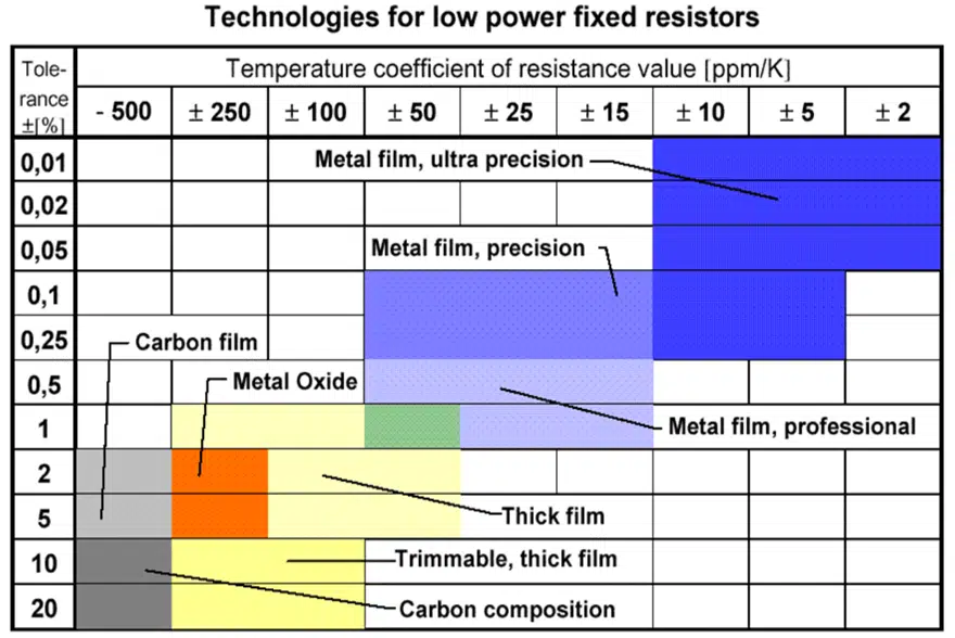
Typical commercial tolerance ranges by technology:
- Thick film: about ±1% to ±5% (some series to ±0.5%).
- Thin / metal film: about ±0.1% to ±1%, with precision series down to ±0.05%.
- Metal foil: down to the order of ±0.005% to ±0.1%.
- Carbon film: typically ±2% to ±5%; carbon composition is usually wider.
- Metal element shunts: about ±1% to ±5%; specialized precision series can be tighter.
- Wirewound: often ±1% to ±5%; precision types can be much better.
Choose the highest tolerance that still meets your error budget; overly tight tolerances add cost and can strain supply chain.
Temperature coefficient of resistance (TCR)
Typical TCR classes and application guidance:
- Ultra‑precision and metrology
- Metal foil down to a few ppm/°C.
- Premium thin‑film resistors around ±5…±10 ppm/°C.
- Precision analog and instrumentation
- Thin/metal film in the ±10…±25 ppm/°C region.
- High‑grade thick film and some metal film at ±25…±100 ppm/°C.
- General purpose and cost‑sensitive
- Standard thick film, metal oxide and carbon film around ±100…±300 ppm/°C or higher.
Strongly non‑linear TCR (such as some carbon composition) complicates error budgeting and should usually be avoided in new precision designs.
Tracking and matching
In many circuits, ratio stability matters more than absolute value:
- Use matched networks or arrays (thin‑film or thick‑film networks, or foil networks at the very high end) when:
- Setting gain in precision op‑amp stages.
- Building bridge circuits or ratio dividers.
- Driving differential ADC inputs or reference ladders.
- For moderate‑precision digital functions (pull‑ups, series terminations, logic biasing), thick‑film arrays often provide enough matching at low cost.
Stability and drift over time
- Thick film
- Moderate drift; expect several 0.1% over long‑term life at rated stress.
- For precision circuits, derate power and keep temperature and moisture well controlled.
- Thin / metal film
- Superior stability; long‑term drift can be kept below 0.1% with conservative derating.
- Often selected for precision industrial and instrumentation designs.
- Metal foil
- Exceptional long‑term stability with only tens of ppm drift.
- Suited for calibration standards and very demanding measurement equipment.
1.3 Step 3 – Define Environment (Temperature, Humidity, Application Class)
Environment determines how you balance robustness versus precision.
Temperature
- Standard commercial and industrial
- Datasheets often specify rated power at 70 °C with linear derating to max temperature (125–155 °C for many chips).
- In high‑reliability designs, keeping hot spot ≤125 °C significantly improves life.
- High‑temperature applications
- Metal oxide, some wirewound and metal element resistors can withstand elevated hot‑spot temperatures up to around 250–275 °C, depending on the series.
- Coating and lead‑wire materials must also support the environment.
Humidity and contamination
- Moisture robustness
- Thick film and metal glaze/metal oxide resistors are relatively robust, due to glass and ceramic matrices.
- Very thin metal films and ultra‑high‑value resistors can be sensitive to humidity and require protective coatings or special constructions.
- Sulphur and corrosive atmospheres
- Use sulphur‑resistant chips and terminations, or coated/high‑reliability versions.
- Consider conformal coating on the PCB where appropriate.
Automotive, industrial, and harsh environments
- Automotive and heavy industrial
- Prefer AEC‑Q200‑qualified thick film chips for generic biasing and pull‑ups.
- Use AEC‑Q200 metal element shunts in current sense positions.
- Metal oxide or thick‑film surge resistors for load dump, relay drive, and other stress points.
- Laboratory, metrology, and medical
- Thin film and metal foil resistors in sensitive analog paths.
- Optional hermetic packages or multi‑layer lacquer coatings for long‑term drift control and cleanliness.
Automotive Qualification and Reliability (AEC‑Q200)
In automotive and other high‑reliability applications, resistor selection is strongly influenced by AEC‑Q200, the Automotive Electronics Council stress‑test qualification standard for passive components. AEC‑Q200 defines a series of environmental, mechanical, and electrical stress tests (temperature cycling, high‑temperature storage, humidity bias, load life, vibration, etc.) that manufacturers use to qualify specific product families across defined service‑temperature grades.
It is important to note that AEC‑Q200 is a qualification framework rather than a formal “certification”: there is no central authority issuing certificates, instead manufacturers document that a given series has passed the relevant AEC‑Q200 test matrix. For safety‑relevant or mission‑critical functions, always verify that the selected resistor series is qualified to the AEC‑Q200 grade matching your worst‑case ambient and hot‑spot temperatures.
In practice, reliability‑driven selection benefits from a simple checklist:
- Confirm AEC‑Q200 qualification (and grade) for automotive or similar harsh use cases.
- Derate continuous power to roughly 50–70 % of the rated value to control long‑term drift.
- Check load‑life drift rather than only initial tolerance, and include it in the error budget.
- Review moisture, sulfur, and contamination robustness for exposed locations.
- For current‑sense positions, prefer metal element shunts and ensure robust PCB copper heatsinking and Kelvin connections.
1.4 Step 4 – Define Cost, Volume, and Assembly Constraints
Now select the cheapest technology that still satisfies all electrical, accuracy, and environmental constraints.
Relative cost ladder (typical)
From lowest to highest cost, in broad terms:
- Thick‑film chip resistors and thick‑film arrays.
- Carbon film (mainly legacy THT, sometimes still economical).
- Standard metal film (axial, MELF).
- Thin‑film chip resistors and precision networks.
- Metal element shunts (cost‑effective per watt in power paths).
- Metal foil precision resistors.
Actual pricing depends on size, tolerance, TCR, qualification (e.g. AEC‑Q200), and volume.
Assembly and package format
- High‑volume SMT
- Standard chip sizes (0402–1206, and larger for power) in thick film by default.
- Thin film used selectively in precision nodes.
- Chip resistor networks/arrays for dense pull‑ups, terminations, and matched sets.
- Mixed assembly and retrofit
- Axial metal film and carbon film remain common for repairable or manually assembled equipment.
- Metal oxide and wirewound leaded parts populate high‑power or high‑voltage sections.
- Very high power
- SMD or THT metal element, or chassis‑mount wirewound resistors.
- Include mechanical mounting, heatsinking, and creepage/clearance in the design.
Beyond the per‑piece price, long‑term availability and second‑sourcing should also influence technology choices. Mainstream chip resistor technologies and package sizes (for example 0603 thick film and thin film) are supported by multiple vendors and offer easier multi‑sourcing, while highly specialized constructions (certain foil networks or exotic RF packages) may have limited supplier options and longer lead times. Balancing unique performance against lifecycle and supply‑chain robustness is especially important in automotive, industrial, and medical equipment.
PCB layout, parasitics, and thermal management
- Layout
- Follow manufacturer land patterns and keep copper balance to avoid tombstoning.
- Respect creepage for high voltage and clearance around hot parts.
- Parasitics
- For high‑speed or RF circuits, minimize loop area and via inductance.
- For very low‑value shunts, use Kelvin connections and low‑inductance geometries.
- Thermal
- Place power resistors where airflow and copper spreading are sufficient.
- Avoid clustering hot components that might locally raise temperature well above ambient.
Modelling and Simulation of Resistor Parasitics
For high‑speed, RF, and precision current‑sensing applications, it is increasingly useful to include realistic resistor models in circuit and field simulations. At minimum, low‑value shunts and HF terminations should be represented by an R‑L‑C macromodel that reflects the manufacturer’s typical parasitic inductance and capacitance for the specific package and value.
Many high‑frequency thin‑film and RF‑optimized resistor series are supplied with broadband S‑parameter files, which can be used directly in RF circuit simulators or EM tools. For very low‑ohmic metal strip shunts, the PCB copper and Kelvin sense routing form an integral part of the resistor system and should be considered in thermal and electrical simulations, particularly in high‑current power converters and automotive traction inverters.
2. Technology Comparison and Benchmark Tables
The most common resistor technologies includes thin film, thick film, wirewound or MELF constructions.

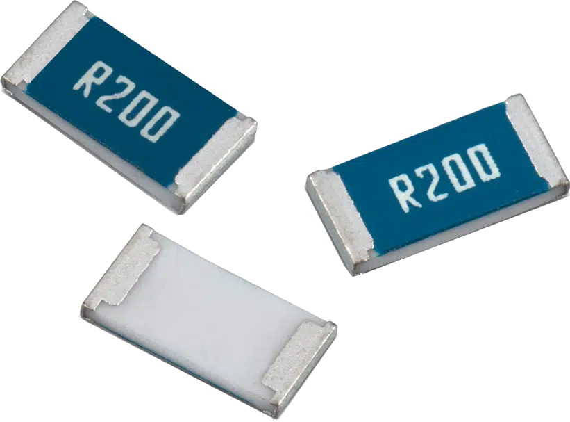
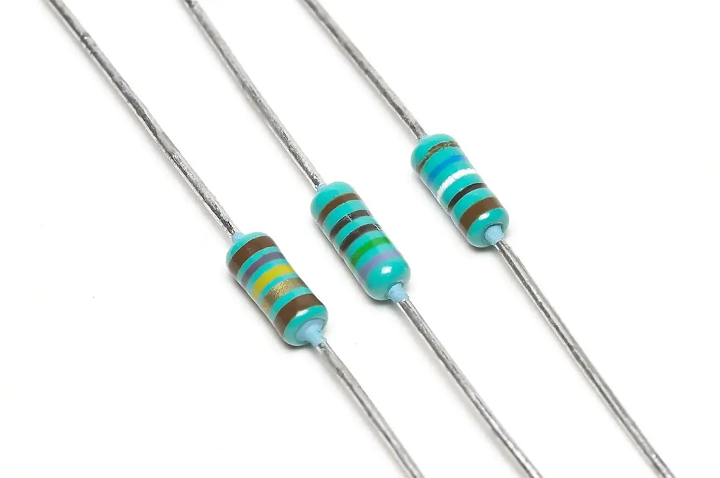
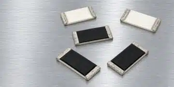
As with the other resistor technologies, thick- and thin-film resistors offer unique sets of cost/performance tradeoffs (Table 1). Metal film chip resistors are low-cost in high quantities and have excellent frequency response with low inductance. They are suited for applications that involve MHz operating frequencies and μs rise times.

Voltage Dependence
If we apply a voltage on a resistor it’s resistance will drop slightly in certain types. Therefore the resistance change is negative. The change per volt of applied voltage is called voltage coefficient, VC, and is expressed in %/V or better, μV/V. The coefficient is determined not only by the resistive material but also by the dimensions, i.e., the electrical field strength, and the time of applied voltage. Thus, MIL-STD-202, Method 309 prescribes measurements when the voltage is applied intermittently for less than 0.5 seconds. Two measurements is performed: the resistance (r) at 0.1 x rated voltage (VR) and the resistance (R) at 1.0 x VR. The voltage coefficient, VC, then is computed as:
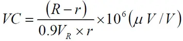
If we disregard pure metallic resistive elements common values of the voltage coefficient are between –10 and –100 μV/V. The voltage dependence is negligible for resistance values below 1000 ohms.
An evident voltage dependence combined with AC voltages will cause distortion and a third harmonic attenuation.
Frequency Dependence
A resistor has a certain parasitic degree of both capacitance and inductance. Between the turns there is a certain capacitive connection. Inductance appears already in a straight lead, approximately 1 nH/mm of length but is amplified by the coil action from windings and spiraled patterns. In carbon composition resistors only capacitance emanating from the multitude of parallel current paths manifests itself.
Figure 2. shows the equivalent circuit being simplified to models for high and low resistance values.
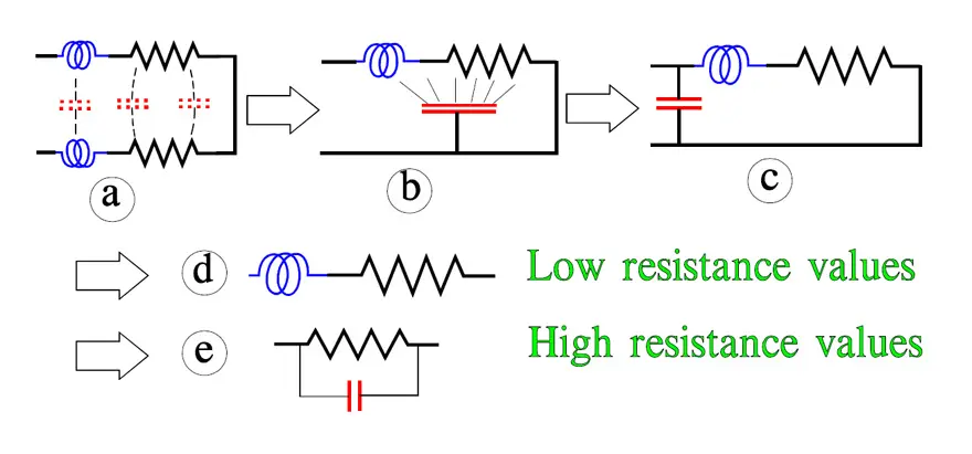
- a) Small sizes
- b) low R-value
- c) Chip design
- d) Small or no lead wire (SMD)
- e) Even body
The frequency dependence of resistance decreases if the resistors:
- have small dimensions.
- have a low resistance value.
- are of a thin film design. Even a thick film design is favorable.
- have as short a lead as possible, like SMDs.
- are geometrically even, i.e., without sudden geometrical changes along the resistor body.
How the frequency dependence may influence the impedance is shown in Figure 3.
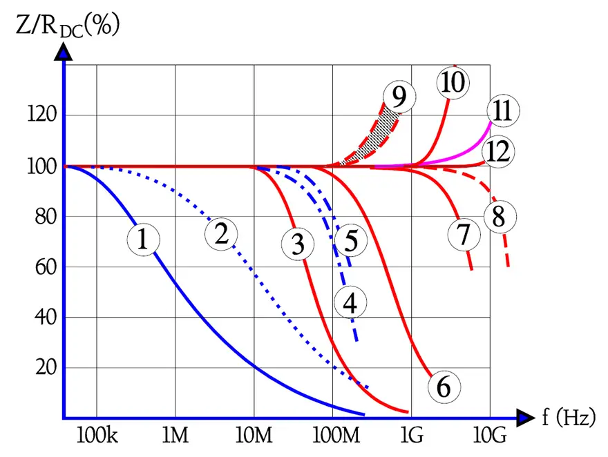
Carbon composition, ¼ W, 1 MW.
- Carbon composition, ¼ W, 100 kW.
- Chip, thick film, EIA size 0603, 100 kW; c » 0.05 pF; L » 0.4 nH.
- Metal glaze or metal film, DIN size 0207, 100 kW; c » 0.4 pF.
- MELF, DIN size 0204, 10 kW.
- Chip, thick film, EIA size 0603, 10 kW; c » 0.05 pF; L » 0.4 nH.; Chip, metal foil, EIA size 1210, 10 kW.
- Chip, thick film, EIA size 0603, 1 kW; c » 0.05 pF; L » 0.4 nH.
- MELF, DIN size 0102, high frequency design, 10 W; c » 0.035 pF; L » 0.8 nH.
- MELF, DIN size 0204, 10 W.
- Chip, thick film, EIA size 0603, 10 W; c » 0.05 pF; L » 0.4 nH.
- Chip, thin film, EIA size 0603, 100 W; c » 0.035 pF; L » 1.2 nH.
- Chip, thick film, EIA size 0603, 100 W; c » 0.05 pF; L » 0.4 nH.
The examples in Figure 3 represent typical behaviors taken from major manufacturers’ datasheets and serve as a guide rather than exact specifications. They illustrate how resistance value, body size, and technology influence parasitic L and C and therefore the AC impedance versus DC value.
For practical design work, a few simple rules of thumb are usually sufficient:
- Smaller SMD resistors with short terminations (especially thin film) behave closest to ideal resistors up into the high‑MHz range.
- Very low‑value film and metal element resistors tend to be slightly inductive at high frequency, while very high‑value parts become dominated by parasitic capacitance.
- Carbon composition and older leaded parts (spiral‑cut metal film, wirewound) show strong frequency dependence and should be avoided in modern high‑speed or RF signal paths.
- High‑frequency optimized chip resistors are characterized with impedance‑versus‑frequency or S‑parameters and should be treated as RF components in simulation and layout.
The examples in Figure 2. represent a guide only. They are taken from major manufacturers’ data sheet. Note how the resistance value of an otherwise equivalent component influences the parameters: No. 3, 6, 7, 10 and 12. Another example, No. 8, shows a MELF component that, by means of a specific spiraling technique, is given excellent high frequency characteristics. Generally the frequency dependence of the different resistor materials can be divided into three groups:
| Technology | Frequency Dependence |
| Carbon composition | high |
| Metal glaze, cermet, thick film | moderate to low |
| Metal film, metal oxide and carbon film | low |
Film resistors may approximately be classified as follows:
- values < 100Ω are inductive.
- values between 100 and 470Ω are practically true resistive.
- values above 470Ω are capacitive.
Thin Film Chip High Frequency Resistors
As the industry extends products above the GHz range (5G), an understanding and improvement of resistors especially in thin films products’ performance needs to be considered.
Performance of thin film resistors at high frequency is dependent on the case size, trim method, part value and termination style. The reduction in parasitic impedance for smaller cases sizes is consistent with the smaller landing pads and device dimension.
Termination style:
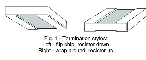
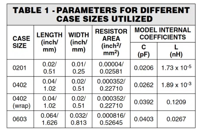
The large change between 0201 and the 0402 and 0603 can be related to significant reduction in maximum resistor area. The ratios of the maximum areas for the resistors by case size (0603 : 0402 : 0201) are 1 : 2.32 : 20.4. The small change in device area for the 0402 and 0603 case sizes is most likely related to the small differences and occasional reversal in the device performance.
In the RF and microwave domain, “generic” thin‑film chip resistors are often sufficient up to a few GHz, but for 5G FR2 and mmWave applications there are dedicated high‑frequency thin‑film series specified up to 50–70 GHz. These parts are supplied with broadband impedance or S‑parameter data and use optimized geometries (for example edge‑cut or flip‑chip terminations) to minimize parasitic inductance and capacitance over a wide band.
Because of this, high‑frequency chip resistors must be treated as RF structures rather than ideal lumped elements. A practical design workflow is:
- Define the resistor’s RF role (e.g. termination, attenuator element, bias feed) and target frequency band.
- Select candidate parts based on published impedance‑versus‑frequency curves or S‑parameter files and required return loss.
- Include the vendor model or S‑parameters in circuit and/or EM simulation using the actual PCB stack‑up and launch geometry.
- Verify in hardware by measuring insertion loss and return loss (S‑parameters) on the intended layout.
This approach keeps the resistor behavior under control even at tens of GHz and avoids surprises when transitioning from schematic‑level design to real boards.
Technology Benchmark Table
The following table compares the major resistor technologies for typical low‑ to mid‑power general‑purpose applications. Values are indicative ranges, not tight specifications.
| Attribute | Thick film | Thin / metal film | Metal foil | Wirewound | Carbon film | Metal oxide / glaze |
|---|---|---|---|---|---|---|
| Cost level (relative) | Very low | Medium | Very high | Medium | Low | Low–medium |
| Typical resistance range | ~1 Ω to 100 MΩ+ | ~1 Ω to 20–50 MΩ | ~1 Ω to 100 kΩ (typical precision range) | ~10 mΩ to 100 kΩ | ~10 Ω to 10 MΩ | ~1 Ω to 100 MΩ |
| Typical power range (single part) | 0.05–1 W (chips) | 0.05–0.6 W (chips, MELF) | 0.05–0.6 W (specialized precision) | 0.5–50 W+ (chassis types) | 0.25–2 W (axial) | 0.25–5 W (axial, power types) |
| Tolerance brackets (typical) | ±0.5…±5% | ±0.05…±1% | ±0.005…±0.1% | ±0.1…±5% | ±2…±5% | ±1…±5% |
| TCR brackets (typical) | ~±100…±300 ppm/°C | ~±5…±50 ppm/°C | ~±0.2…±5 ppm/°C | ~±10…±100 ppm/°C | ≥±200 ppm/°C | ~±100…±300 ppm/°C |
| Noise | Medium–high | Low | Very low | Very low | High | Medium |
| Long‑term stability | Medium | Good | Excellent | Good–excellent | Fair–poor | Good |
| Pulse/surge capability | Good (surge‑rated very good) | Limited | Limited | Very good (energy) | Good | Very good (especially power types) |
| Package options | SMD chips, networks | SMD chips, MELF, networks | SMD, special leaded | Leaded axial, radial, chassis‑mount | Leaded axial | Leaded axial, power, some SMD |
| HF behavior | Good in chip format | Very good in chip format | Good in suitable packages | Inductive at high f | Moderate | Moderate |
Specialized Technologies for High‑Frequency and Current Sense
The next table summarizes specialized resistor technologies that are not fully captured in the general‑purpose comparison but are critical for RF/microwave and high‑current applications. Values are indicative ranges.
| Attribute | RF‑optimized thin‑film chip | Metal strip / metal element shunt | Precision metal foil network |
|---|---|---|---|
| Typical role | RF termination, attenuator element, bias feed at GHz frequencies | DC and low‑frequency current sensing in power paths | Ultra‑stable precision dividers and gain networks |
| Frequency range | DC up to 20–70 GHz (depending on series) | DC to hundreds of kHz (some designs usable into MHz with low inductance) | DC to low MHz (primarily precision analog) |
| Typical resistance range | ~10 Ω to 1 kΩ (terminations) and wider for biasing | ~0.2 mΩ to a few 100 mΩ | ~100 Ω to 100 kΩ per element (ratio‑focused) |
| Parasitic behavior | Very low L and C, characterized with S‑parameters | Very low inductance when designed with wide, flat geometry; some thermoelectric effects | Low parasitics; optimized for stability rather than extreme HF performance |
| Tolerance / TCR | Tolerance down to ±0.1–±1%; TCR typically 5–50 ppm/°C | Tolerance around ±0.5–±5%; TCR from a few ppm/°C (precision types) to 100+ ppm/°C | Tolerance down to ±0.005%; TCR as low as a few ppm/°C with excellent tracking |
| Power handling | Low to moderate per chip; limited by small footprint and RF heating | Very high power‑per‑volume; several watts in compact packages with good cooling | Low to moderate; focus is on precision rather than wattage |
| Typical qualification | Often available in AEC‑Q200 variants for automotive RF/telecom | Widely available in AEC‑Q200 automotive and industrial series | Selected series qualified for industrial or instrumentation; automotive use is niche |
3. Use‑Case‑Based Recommendations
This section gives quick design‑time guidance. In each case, first verify that basic electrical and environmental limits are satisfied (Sections 1.1–1.3), then choose from these shortlists.
3.1 Precision ADC Front‑End
Example circuits: input filters, gain‑setting resistors, reference dividers, sense resistors near ADC input.
- Prefer
- Thin‑film chip resistors for input and feedback networks.
- Thin‑film or foil networks where ratio matching dominates error.
- Metal foil resistors in extremely demanding metrology or calibration systems.
- Avoid
- Standard thick film for critical gain‑ or offset‑sensitive positions (due to higher TCR, noise, and drift).
- Carbon film and metal oxide for anything beyond low‑precision biasing.
3.2 Precision Operational Amplifier Gain Stages
- Prefer
- Thin‑film chip or network resistors with low TCR and tight tolerance for feedback and gain‑setting resistors.
- Metal foil for ultra‑stable references or long‑term drift‑critical applications.
- Avoid
- Mismatched or dissimilar technologies in the same gain‑defining network.
- Thick film in precision instrumentation stages unless all error sources are carefully budgeted and compatible.
3.3 Cheap Consumer Logic Board
Example circuits: microcontroller boards, power‑supply housekeeping, pull‑ups/pull‑downs, LED series resistors.
- Prefer
- Standard thick‑film chip resistors for almost all biasing and logic functions.
- Thick‑film arrays for dense pull‑up and termination banks.
- Consider
- Thin film only in a few specific points if you need slightly better analog performance and the cost is justified.
- Avoid
- High‑end foil or precision thin‑film parts unless they solve a specific problem; they will not pay back in typical consumer products.
3.4 High‑Power Shunt for Current Measurement
Example circuits: DC bus current sensing, battery monitoring, inverter phase sense, automotive current measurement.
- Prefer
- Metal element (shunt) resistors, SMD or through‑hole, with known TCR and good PCB copper heatsinking.
- Wirewound power resistors for lower‑frequency applications where inductance is acceptable.
- Avoid
- Regular thick‑film resistors for primary current‑shunt functions if significant power is dissipated or accuracy is important.
- Carbon film for high currents or where thermal EMFs and drift matter.
Metal Strip and Specialized Current Sense Resistors
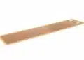
For high‑current measurement in power electronics, automotive, and battery systems, metal strip (metal element) current sense resistors have become a primary technology choice. They offer very low resistance values from the single‑milliohm range up to a few tens of milliohms with excellent power‑per‑volume and relatively low inductance when designed with suitable geometries and Kelvin terminals.
Compared with thick‑film shunts, metal strip resistors typically provide better long‑term stability, lower TCR, and more predictable thermal behavior, at the expense of a more limited resistance range and slightly higher component price. They are therefore the default choice for DC bus current sensing in EV/HEV traction inverters, on‑board chargers, DC fast chargers, and high‑current industrial drives, where a combination of accuracy, power handling, and AEC‑Q200 qualification is required.
When using metal strip shunts:
- Treat the PCB copper as part of the resistor and model its contribution to resistance and temperature rise.
- Use true Kelvin sense routing for measurement leads to avoid including high‑current path voltage drops.
- Place the part so that heat can spread into wide copper areas and, where needed, into heatsinks or baseplates.
3.5 High‑Voltage Divider
Example circuits: mains and kV measurement, PFC and SMPS monitoring, insulation testers.
- Prefer
- High‑value metal oxide, metal glaze or thick‑film HV resistors, often used in series chains for better voltage distribution.
- Wirewound or rod‑type resistors where lower values and better surge tolerance are necessary.
- Avoid
- Thin film at the extreme high‑voltage end unless specifically designed and rated for HV.
- Single large‑value resistors operated close to their maximum voltage rating without margin.
3.6 Surge‑ and Pulse‑Robust Snubber or Inrush Resistor
Example circuits: relay inrush limiting, motor starter, snubbers across switches, surge paths.
- Prefer
- Surge‑rated thick‑film or MELF resistors, metal oxide, and metal glaze types.
- Wirewound power resistors where energy content is high and space/heatsinking is available.
- Avoid
- Thin‑film resistors that are not specifically pulse‑rated.
- Small SMD chips operated near their power limit under repetitive surges.
3.7 RF, High‑Speed Logic Termination, and Matching
- Prefer
- Thin‑film SMD resistors with low parasitics for RF matching, terminations, and attenuators.
- SMD thick‑film resistors for less critical HF nodes and digital terminations.
- Avoid
- Large leaded wirewound or carbon film parts in high‑frequency paths (inductance and parasitics).
3.8 Automotive and Harsh Industrial Control
- Prefer
- AEC‑Q200‑qualified thick‑film chips for generic biasing and digital functions.
- AEC‑Q200 metal element shunts for current sensing.
- Metal oxide or thick‑film surge resistors in positions exposed to load dump and relay transients.
- Avoid
- Non‑qualified parts in critical safety or high‑reliability functions.
- Technologies with poor moisture or contamination robustness in exposed areas.
4. Conclusion
Resistor technology selection is best approached systematically: first verify that candidate technologies survive the electrical, environmental, and assembly constraints, then refine the choice based on accuracy, stability, and cost. Thick‑film chips cover most cost‑sensitive, general‑purpose uses, while thin‑film and metal foil resistors dominate precision analog and metrology, and metal element shunts, wirewound, and metal oxide/glaze parts fill the high‑power, high‑voltage, and surge‑critical niches.
By combining the four selection steps with the benchmark tables and the use‑case‑oriented recommendations in this guide, designers can converge quickly on the most appropriate resistor technology and package for each circuit function and operating environment.
FAQ
For gain‑setting, feedback, and reference divider resistors around an ADC, thin‑film chip resistors are usually the best compromise between precision, low noise, and cost. Metal foil resistors are reserved for extremely demanding metrology‑grade systems where cost and size are less critical.
Metal strip (metal element) current sense resistors are preferred whenever you need accurate low‑ohmic values with good TCR, high power‑per‑volume, and stable long‑term behavior, such as in DC bus sensing of power converters, EV traction inverters, and battery management systems. Thick‑film shunts are suitable mainly for lower accuracy or lower power applications.
Standard thick‑film chips work well for many MHz‑range digital terminations and non‑critical RF nodes, but for precision matching, low reflection, or operation into the multi‑GHz or 5G/mmWave range you should choose thin‑film or dedicated RF‑optimized resistor series with specified impedance‑versus‑frequency or S‑parameter data.
Not every resistor in an automotive system must be AEC‑Q200 qualified, but components in safety‑relevant, high‑stress, or long‑lifetime positions should come from AEC‑Q200‑qualified series at an appropriate grade. For non‑critical infotainment or convenience functions, standard industrial‑grade parts may be acceptable depending on OEM requirements.
How to Select a Resistor Technology in 5 Steps
- Step 1 – Check basic electrical stresses
Determine required resistance range, continuous power, maximum working and surge voltage, pulse profile, and frequency/bandwidth. Exclude any technologies that cannot survive these stresses.
- Step 2 – Define accuracy and stability requirements
Set targets for tolerance, TCR, matching/ratio accuracy, and long‑term drift based on your error budget. This step usually decides between thick‑film, thin‑film, foil, and metal element shunts.
- Step 3 – Consider environment and qualification
Identify ambient and hot‑spot temperatures, humidity, contamination, and whether automotive or similar high‑reliability standards (such as AEC‑Q200) apply. Prefer qualified series for harsh or safety‑relevant applications.
- Step 4 – Choose package and assembly format
Decide between SMD chips, arrays, MELF, axial, or power/chassis‑mount packages based on assembly method, available space, creepage/clearance, and thermal management options.
- Step 5 – Optimize for cost and supply chain
Among the technologies that pass the first four steps, select the lowest‑cost option with acceptable second‑sourcing and lifecycle prospects. Use the benchmark tables and use‑case recommendations in this article as a final sanity check.
References
- Thin Film Resistor Design Guide
- For selection and application of thin‑film and metal‑film resistors in precision analog and RF circuits.
- Focus points: tolerance/TCR selection, matching, noise, long‑term stability.
- Thick Film Resistor Design Guide
- For thick‑film chip and array design, including derating, pulse capability, layout recommendations, and automotive considerations.
- Fundamentals of Types and Construction
- For a comprehensive overview of resistor construction principles, materials, and how structure drives performance (noise, pulse behavior, TCR, stability).
- Other Resistor Technologies: Carbon, Metal Element, Metal Oxide, Metal Foil, Conductive Plastic
- MELF Resistors
- Wirewound Resistors