


This article based on Würth Elektronik webinar by Andreas Dreher explains PCN Test Methods and how to inspect Quality and Reliability of PCB boards.
Key Takeaways
- The article explains PCN Test Methods for assessing the quality and reliability of PCB boards.
- PCBs are complex systems requiring precise control over various manufacturing processes to ensure quality.
- Inline process control, chemistry monitoring, and quality gates are crucial for detecting defects early.
- Advanced laboratory techniques like TMA, FTIR, and reliability testing enhance PCB robustness and longevity.
- Engaging with manufacturers early to discuss design requirements and testing can improve yield and reliability.
Introduction
Printed circuit boards (PCBs) are often treated as a commodity component, selected late in the design process and purchased mainly on cost and lead time. In reality, the PCB is a highly engineered system element whose quality and long‑term reliability depend on a complex chain of processes, inline monitoring, dedicated quality gates, and advanced laboratory methods. Many of these measures remain invisible to end customers, yet they determine whether a design will be robust in production and stable in the field over many years.
For designers of power electronics, sensor interfaces, and high‑reliability assemblies, PCB quality is as critical as the choice of capacitors, inductors, resistors, and connectors. This article – part of the “ABC of PCB Interconnect” knowledge series on Passive Components Blog – explains how manufacturing, test methods, and reliability engineering for bare PCBs directly influence the performance and lifetime of your passive components and solder joints in the finished assembly.
This Würth Elektronik presentation and article provides a structured overview of PCB process control and reliability assurance, from raw material handling through inline chemistry control, AOI and X‑ray alignment, electrical test, microsections, and advanced long‑term reliability tests such as climatic chambers and interconnect stress testing (IST). The goal is to equip engineers, quality managers, and purchasers with a deeper understanding of what “quality” really means for PCBs, and how to translate application requirements into meaningful specifications and documentation.
1. PCB Manufacturing Process Overview
PCB manufacturing is a multi‑stage process where each step introduces potential variation and failure mechanisms. Even a “simplified” process flow already involves numerous chemical, mechanical, and optical operations that must be controlled within tight tolerances to guarantee consistent quality.
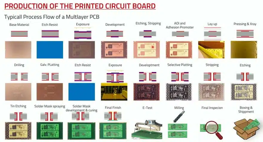
1.1 From raw material to inner layers
The process starts with copper‑clad laminate, typically FR‑4 sheets with copper foil on one or both sides. A photosensitive resist (dry film or liquid) is laminated onto the copper surface, exposed through artwork using strong UV light, and developed so that:
- Exposed areas: Cure and remain on the copper as etch resist.
- Unexposed areas: Stay soft and are removed in development, exposing bare copper.
The exposed copper is then etched away, the resist stripped, and the result is a patterned inner layer. Several such inner layers are produced and later stacked and pressed into a multilayer structure. Already at this stage, process stability in lamination, exposure energy, development, and etching directly influences conductor width, spacing, and uniformity of copper thickness.
1.2 Multilayer lamination, drilling, and plating
Inner layers are combined with prepregs and outer copper foils in a defined stackup and pressed under temperature and pressure. During lamination, the FR‑4 resin softens, flows, and cures, while glass fibers and copper structures restrict and shape the movement. This can cause shifts of inner layers, warpage, and thickness variations. After pressing, the multilayer appears as a featureless copper sheet, with all inner structures buried inside.
Next, through‑holes and vias are drilled and the holes are metallized (galvanic plating) to create conductive barrels. To reduce copper waste, pattern plating is often executed in two steps with different resists, so that additional copper is only built up where needed for tracks and pads, rather than plating the entire panel and etching away up to 70% of the copper. This approach balances material cost and process complexity while providing the required current‑carrying capability and reliability.
1.3 Solder mask, final finish, and panelization
Once the copper pattern is defined and plated, solder mask is applied (typically by spraying or curtain coating), developed, stripped of unwanted areas, and cured. Final surface finishes are then deposited on exposed copper pads, such as electrolytic nickel‑gold (ENIG), to provide solderability, corrosion resistance, and wire bonding capability where required. At this point the PCB is electrically functional and can, in theory, be tested.
In practice, tests are usually performed after solder mask and final finish, because many defects are related to these layers or only become relevant once the full layer stack is complete. The last mechanical step is milling or routing (and V‑cut where used), followed by final inspection, documentation, and packaging.
1.3.1 Common surface finishes and their implications
Different applications benefit from different PCB surface finishes. Besides ENIG, several alternatives are widely used, each with its own strengths and weaknesses in terms of solderability, reliability, and cost.
| Finish type | Typical use cases | Strengths | Limitations / risks |
|---|---|---|---|
| ENIG (Ni/Au) | Fine‑pitch SMT, BGAs, wire bonding | Very flat, good solderability, long shelf life | Risk of “black pad” if poorly controlled, higher cost |
| Immersion silver | High‑speed / RF, fine‑pitch SMT | Flat surface, good conductivity, low contact resistance | Sensitive to handling and sulfurous atmospheres |
| Immersion tin | General SMT, press‑fit connectors | Flat, good solderability, good for press‑fit pins | Tin whisker risk if not well controlled, storage sensitivity |
| HASL / LF‑HASL | Robust industrial, through‑hole, mixed tech | Robust, cost‑effective, tolerant to multiple soldering cycles | Less planar, less suitable for very fine‑pitch or tight coplanarity |
2. Inline Process Control And Chemistry Monitoring
A significant part of quality assurance happens “invisibly” inside the process lines. Modern PCB manufacturing plants rely heavily on inline monitoring to stabilize chemistry, temperature, and mechanical parameters, long before any formal quality gate is reached.
2.1 Horizontal process lines and modules
Many wet processes such as cleaning, micro‑etching, etching, and rinsing are implemented in horizontal conveyorized lines. Boards are fed on rollers and pass through different modules that each perform a specific function. Typical module types are:
- Spray modules: High‑pressure nozzles spray chemistry intensely onto the board. This is critical for etching, where fresh chemistry must constantly reach the copper surface to achieve uniform and predictable etch rates.
- Dwell modules: Boards are immersed or exposed to liquid with minimal movement for a defined dwell time (e.g., 180 seconds or more), allowing slower reactions or conditioning processes to take place.
- Rinse modules: Cascade rinses with fresh or deionized (DI) water between chemical stages prevent cross‑contamination and remove residues after each process. Final rinses and drying ensure no active chemistry remains on the PCB surface.
2.2 Online monitoring of critical parameters
Each chemical module has key parameters that must remain within defined limits to ensure stable output. Typical monitored parameters include:
- Chemistry concentration: Affects etch rate, plating rate, and surface conditioning quality.
- pH value: Influences reaction kinetics and copper surface quality.
- Temperature: Strongly affects reaction speed and stability of additives.
- Spray pressure and distribution: Non‑uniform pressure results in non‑uniform etch or clean, leading to local over‑ or under‑etching.
Process control systems often visualize these parameters as trend charts with a target value (green line), acceptable process window (orange band), and limit thresholds (red lines). Automatic replenishment adds chemistry to keep the process within the orange band. If values exceed orange limits, operators are alerted to diagnose issues such as missing replenishment or sensor malfunction. Crossing red limits typically causes the line to block new boards and sort boards inside the machine for later review.
For PCB designers, the size of the process window in these controlled parameters translates directly into achievable minimum line/space and yield. Relaxed design rules (for example, using 100–125 µm instead of 75–100 µm where space allows) give the fabricator more headroom to keep all boards inside the ideal “orange band” of their control charts and reduce the risk that small process drifts lead to scrap or marginal quality.
2.3 Laboratory verification and sensor validation
Inline sensors can drift, clog, or fail mechanically. To ensure that online readings remain trustworthy, a dedicated in‑house chemistry lab performs regular analyses of process baths and control samples from each machine. Some measurements (e.g., complex titrations, trace contaminations, special additive concentrations) cannot be measured online and therefore rely on lab methods. This dual approach — inline monitoring plus offline lab verification — is a cornerstone of robust process control and is often underestimated by customers who only see final certificates and inspection reports.
3. Quality Gates And Formal Inspection Methods
On top of inline control, dedicated quality gates are introduced at critical stages of the process. These gates use specific test and inspection methods to detect defects that may not be visible or accessible later in the process, such as inner layer shorts or opens sealed inside the multilayer.
3.1 Automatic optical inspection (AOI) for inner layers
Inner layer AOI is performed after pattern etching and resist stripping, before lamination. A high‑resolution camera scans the copper pattern using multiple light colors (white, blue, red, etc.) to optimize contrast for different defects and residues. The system compares the scanned image to the original Gerber data, which for inner layers is essentially a black‑and‑white representation:
- Copper: Highly reflective, appears bright or white.
- Base material (FR‑4): Non‑reflective, appears dark.
Typical AOI resolutions are around 25 µm, enabling detection of fine opens, shorts, nicks, and other pattern defects. Repair of inner layer defects is usually not performed due to feature size and the risk of unreliable rework. Instead, the focus is on “right first time” production and scrap of defective inner layers.
3.2 IPC acceptance criteria and customer‑specific limits
AOI and final inspection often rely on IPC standards such as IPC‑A‑600 / IPC‑6012. These allow certain local reductions in conductor cross‑section (e.g., due to small nicks or dimples) while still passing the board as compliant, based on built‑in safety margins in current‑carrying capacity calculations. For example, if a track is already at the lower end of its allowed width and loses an additional fraction of cross‑section due to a small defect, the IPC rules may still consider it acceptable.
However, some customers expect a more conservative interpretation and may be surprised when AOI exposes “defects” they deem critical but are still IPC‑acceptable. In such cases, customer‑specific test parameters and acceptance criteria should be agreed. This includes stricter rules for minimum conductor width, allowed nicks, and minimum separation to ground planes or copper pours. Good design practice also helps: where space allows, increasing clearances (e.g., from 75 µm to 100–150 µm around pads) significantly improves yield and reduces sensitivity to data conversion and rasterization artifacts.
IPC classes provide a useful baseline for defining how much deviation from nominal is acceptable, but they do not automatically guarantee that every application‑specific risk is covered. In practice, most industrial and consumer products are built to IPC Class 2, whereas safety‑critical automotive, aerospace, and medical designs often require Class 3 or additional customer‑specific requirements on top of IPC.
Examples of where customers may tighten criteria include:
- Minimum annular ring on via pads for high‑reliability connectors and shunt resistors
- Maximum allowed reduction of conductor width in necked‑down trace segments
- Higher minimum insulation distances around high‑voltage or safety‑related nets
Clarifying these points early avoids later discussions when AOI images or microsections reveal features that are IPC‑compliant but not aligned with the end‑customer’s expectations.
3.3 X‑ray alignment and layer registration
After lamination, inner layers are concealed under outer copper. For accurate drilling, X‑ray inspection measures the position of internal targets and vias relative to the panel outline. Composite behavior of FR‑4 (glass fibers and epoxy) during pressing can lead to complex shifting patterns (pillow‑shaped, skewed, etc.). X‑ray systems use image processing and AI‑based algorithms to detect alignment marks and calculate optimal drill offsets so that through‑holes and buried vias hit all target pads.
In an ideal cross‑section, via barrels sit centered in the pads of all layers. In reality, layers may be offset within a specified tolerance. X‑ray measurements on 100% of multilayer panels allow the manufacturer to sort out panels where layer movement exceeds acceptable limits and to maintain process statistics for continuous improvement.
3.4 Electrical test (continuity and isolation)
Final electrical test (ET) is performed after solder mask and surface finish. Finger‑probe or flying‑probe systems contact defined test points and measure:
- Continuity: DC resistance between nodes that should be connected.
- Shorts: Insulation resistance between nodes that should be isolated.
Typical test parameters might include:
| Test type | Parameter | Typical value | Typical IPC limit |
|---|---|---|---|
| Continuity | Test voltage | 10 V | Application‑dependent |
| Continuity | Measurement current | 30 mA | Application‑dependent |
| Continuity | Max resistance (pass) | 10 Ω | Up to 100 Ω allowed |
| Isolation | Min resistance (pass) | ≥ 20 MΩ | Standard IPC values lower |
For high‑reliability or high‑voltage applications, additional high‑potential (hipot) tests can be performed at voltages up to the kV range. However, higher voltages increase test time because the voltage must ramp up and stabilize for each test set. When thousands of nets and several hundred boards are tested, total ET time can easily reach several hours or more than a day for complex products.
3.5 Impedance test coupons and sorting
For controlled‑impedance designs (e.g., differential pairs, high‑speed single‑ended lines), impedance verification is often requested. The PCB panel includes dedicated impedance coupons near the actual product, designed to represent the same stackup, copper thickness, and geometry as the critical traces. After fabrication, the coupons are measured, and a report is generated documenting the measured impedance for each structure.
Impedance testing is a sorting method: coupons within tolerance confirm that the panel process is compliant; coupons out of tolerance indicate that boards from that panel must be scrapped or specially handled. Designers and fabricators should coordinate coupon design closely to ensure coupons truly represent the functional traces, including any copper balancing and reference plane features.
3.6 Design‑for‑Test (DFT) considerations
Electrical test and functional testing are only as good as the access that the layout provides. Good design‑for‑test (DFT) practices make it easier to detect faults early, reduce test time, and avoid false failures caused by marginal test pads or probing conditions.
Key DFT recommendations for bare PCB and in‑circuit testing include:
- Provide dedicated test pads for nets that are not accessible via connectors or component pins, and keep them free of solder mask and silkscreen.
- Observe sufficient clearance around test pads so that fixture pins or flying probes can land reliably without risk of shorting to adjacent copper.
- Avoid placing tall components too close to test pads that must be accessed after assembly, especially on dense mixed‑technology boards.
- Consider the limitations of flying‑probe vs. fixture testing: very fine‑pitch BGAs and stacked HDI structures may require specific pad placement or additional test structures.
- Use solid copper pads for test points rather than thermally relieved pads where possible; thermal spokes can increase contact resistance and lead to apparent “high‑ohmic” failures during continuity testing.
Discussing DFT concepts with the PCB fabricator and the test‑house early in the design phase helps ensure that AOI, electrical test, and functional test coverage are all aligned with the criticality of the application.
4. Dimensional Inspection And Microsections
Microsections and dimensional measurements provide deep insights into the internal structure and mechanical tolerances of the PCB. They are essential for first article inspection (FAI), qualification builds, complaint analysis, and long‑term trend monitoring.
4.1 Microsectioning: methodology and typical measurements
In microsectioning, a small piece of the production board is cut out, embedded, ground with increasingly fine abrasives, and polished to a mirror finish. Under an optical microscope, cross‑sections of vias, tracks, and dielectric layers are visible. Typical measurements include:
- Copper thickness: On inner layers, outer layers, and via barrels.
- Dielectric thickness: Between specific layers, critical for impedance accuracy.
- Solder mask thickness: Especially at track edges and pad edges, important for soldering robustness and insulation.
- Via quality: Barrel uniformity, voids, cracks, pull‑back, resin recession, and inner‑layer connection quality.
Thermal stress can be applied before microsectioning (e.g., solder shock at 288 °C for 10 seconds) to reveal weaknesses such as delamination, barrel cracking, and microvia lifting. Microsections after such stress tests are a powerful tool to validate material selection, lamination parameters, and via processes.
Many of the microsection procedures used in PCB factories follow IPC‑TM‑650 test methods. Referencing the relevant TM‑650 method numbers in specifications or reports helps ensure that both customer and manufacturer have a common understanding of sample preparation, measurement conditions, and acceptance criteria.
4.2 Mechanical tolerances and the V‑cut edge problem
Mechanical tolerances are another area where expectations and physical reality can diverge. FR‑4 is a composite material consisting of glass fibers, epoxy resin, and copper. Defining “the edge” of the board for tolerance measurements can be non‑trivial, particularly in V‑cut panels where the board is partially cut from both sides and later broken out after assembly.
In cross‑section, the V‑groove may show sloping edges, fiber protrusions, solder mask overhang, and resin smearing. Depending on whether an optical (higher sensitivity to debris) or mechanical (contact) measurement is used, the measured edge position can differ. While the middle of the V‑cut is often taken as a practical reference, the only consistent solution is to explicitly define in the drawing what is considered the measurement reference and which measurement method is to be used. Manufacturer and customer must agree on this to avoid disputes over dimensional compliance.
From a reliability perspective, component placement relative to V‑cuts and routing edges is also important. Locating heavy components, connectors, or large capacitors too close to the break‑off edge increases the risk of solder joint cracking during depanelization and in service. Defining a minimum pad‑to‑edge distance in the drawing, and agreeing how this distance is measured, is an effective way to avoid edge‑related failures.
4.3 Documentation packages and reports
Quality documentation can be tailored to the risk level and criticality of the application. Typical document levels include:
- Certificate of compliance (CoC): Confirms that production followed the agreed specifications and standards. Behind this simple document lies a large body of internal records (chemistry logs, AOI data, ET logs, lab reports).
- Inspection certificate: Includes microsections, dimensional measurements, and selected process data. Often used for first series or critical designs.
- First article inspection (FAI) report: Detailed report with extensive measurements of internal and external features. Importantly, the customer must formally approve the FAI to authorize series production.
- Extended or custom reports: For highly critical applications (e.g., aerospace, medical, rail), where additional tests, sampling rates, and reporting formats are defined jointly between customer and manufacturer.
5. Advanced Laboratory Methods And Material Analysis
Beyond routine production testing, modern PCB factories maintain specialized labs for material characterization and forensic analysis. These methods help in incoming material inspection, process optimization, and failure analysis of field returns or test coupons.
5.1 Thermal mechanical analysis (TMA)
Thermal mechanical analysis (TMA) measures changes in sample thickness as a function of temperature. A small PCB sample (e.g., 5 mm × 5 mm) is clamped in a glass fixture, and its thickness is monitored while temperature is ramped up in a controlled profile. Key parameters include:
- Glass transition temperature \(T_g\): The temperature at which the material transitions from a glassy (rigid) to a rubbery state. Below \(T_g\), the coefficient of thermal expansion (CTE) is relatively low; above \(T_g\), CTE increases significantly.
- Time to degradation at high temperature (e.g., T288): Time until failure when the sample is held at a high temperature (e.g., 288 °C). This helps assess the robustness of the resin system during soldering and rework.
CTE behavior is critical because copper has a much lower CTE than FR‑4. When the board is cycled above \(T_g\), the mismatch in expansion between copper and dielectric creates mechanical stress in vias and interfaces. Reducing high‑temperature CTE, increasing \(T_g\), or limiting temperature excursions reduces fatigue and improves long‑term reliability.
To put this into perspective, a board cycled between −40 °C and +125 °C experiences a temperature swing of 165 °C. If the material frequently crosses its glass transition temperature during such cycles, the large change in CTE above (T_g) will significantly increase the mechanical strain on vias and copper‑dielectric interfaces, accelerating fatigue compared with a material whose (T_g) and high‑temperature CTE are better matched to the application.
5.2 FTIR (Fourier transform infrared spectroscopy)
Fourier transform infrared (FTIR) spectroscopy provides a “fingerprint” of organic materials such as resin systems and solder mask. By comparing measured spectra against reference libraries, the lab can:
- Identify material types: Verify whether incoming FR‑4 or solder mask matches the specified system.
- Check composition consistency: Detect changes in formulation or contamination.
- Support failure analysis: Assess whether chemical degradation or contamination has occurred in failed samples.
5.3 Peel strength and adhesion tests
Adhesion between copper and dielectric is a key determinant of delamination resistance and solder pad robustness. Universal testing machines pull copper foils or traces at defined angles and speeds to measure peel strength. Results guide:
- Material selection: Choosing laminates and adhesion promoters.
- Process tuning: Optimizing surface preparation and roughening.
- Design limits: Defining safe pad sizes and shapes for heavy components and connector loads.
5.4 XRF and EDX for plating thickness and composition
X‑ray fluorescence (XRF) equipment measures thickness and composition of metallic layers, such as nickel and gold in ENIG finishes. Gold thickness is often only a few nanometers and cannot be reliably measured in cross‑section. XRF provides non‑destructive verification of:
- Nickel and gold thickness: Conformity to specified ranges.
- Plating uniformity: Across panels and within specific pad groups.
- Elemental composition: In some cases via EDX (energy dispersive X‑ray), supporting investigations of unusual deposits or contamination.
5.5 Thermal imaging and high‑speed electrical characterization
Thermal imaging cameras are used to identify hot spots on powered test boards or coupons. Localized temperature rises indicate excessive current density, poor thermal design, or hidden defects such as high‑resistance joints and partially cracked vias. Once identified, these hot spots can be microsectioned to reveal underlying root causes.
For high‑speed applications, dedicated measurement systems characterize dielectric constant (\(D_k\)) and loss tangent (\(D_f\)) up to tens of GHz. These measurements feed back into impedance control, signal integrity simulations, and material selection for high‑frequency or high‑data‑rate designs.
5.6 Surface finishes and reliability aspects
Surface finishes not only influence solderability and wire‑bonding behaviour, but also play a role in long‑term reliability. Insufficient or excessive nickel thickness in ENIG, for example, can contribute to brittle intermetallics or “black pad” phenomena, while immersion silver and tin are more sensitive to handling, storage, and environmental contaminants. Regular XRF checks of thickness and composition, combined with solderability testing, are therefore key elements of finish‑related quality control.
6. Reliability Testing And Accelerated Life Methods
Reliability testing goes beyond “does it function now?” and asks “how long will it function under real‑world stresses?” Various accelerated tests simulate environmental and thermal stresses, enabling early detection of weak points in materials, stackups, and via structures.
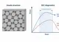
6.1 Climatic chambers and CAF susceptibility
Climatic chambers expose boards or coupons to controlled temperature and humidity conditions, such as:
- 40 °C / 92% RH
- 85 °C / 85% RH
Under applied voltage, these conditions can promote electrochemical migration and conductive anodic filament (CAF) formation between conductors through the glass fiber/resin system. Surface insulation resistance (SIR) tests measure current leakage across the surface, while bulk insulation tests probe through the material. Dendrite growth can occur surprisingly quickly even at low voltages if moisture is present — for instance, a simple experiment with a 10 V supply and a drop of drinking water can produce visible dendrites within seconds, shorting adjacent conductors.
Using dedicated CAF and SIR test boards allows repeatable configuration of conductor spacing, orientation relative to glass fibers, and via structures, simplifying interpretation of results and comparison across materials and processes.
6.2 Thermal cycling and via fatigue
Thermal cycling is one of the most critical stress tests for PCB reliability. Repeated temperature swings cause expansion and contraction of the FR‑4 and copper structures. Because copper and FR‑4 have different CTEs, this creates cyclic mechanical stress, especially in plated through‑holes and microvias. Over many cycles, this can lead to:
- Barrel cracking: Fractures in the via wall along the thickness of the board.
- Inner‑layer separation: Cracks at the interface between barrel and internal pad.
- Microvia lifting: Separation of microvia from its capture pad.
Conventional passive thermal cycling may use two‑chamber systems with an oven (e.g., +125 °C) and cold chamber (e.g., −40 °C). Boards are moved between the two chambers, and resistance is measured periodically. Depending on cycle times and measurement cadence, test durations can extend to weeks or months for high cycle counts.
6.3 Interconnect stress testing (IST)
To obtain faster and more detailed insight, interconnect stress test (IST) systems actively heat dedicated test coupons by passing current through selected via structures. The temperature profile is tightly controlled, and resistance is monitored in short intervals, enabling detection of small changes that precede catastrophic failure. A typical failure criterion might be:
- Failure threshold: Resistance increase of 10% compared to initial value.
IST profiles can simulate operating conditions or solder‑reflow stresses (up to ~260 °C). Once the failure criterion is reached, the coupon is removed and microsectioned to identify the failure mode. By tailoring coupons to reflect actual board designs (e.g., HDI stackups with stacked/staggered microvias, buried vias, and through‑holes), IST provides a highly application‑relevant assessment of interconnect robustness.
6.4 Influence of board thickness on reliability
One striking result from IST and thermal cycling studies is the strong influence of board thickness on via reliability. Consider three boards with identical material, design, and via structures, differing only in total thickness:
| Board type | Nominal thickness | Relative change | Typical cycles to 62% failure |
|---|---|---|---|
| Thick | 2.2 mm | +20% | ≈ 60 cycles |
| Nominal | 2.0 mm | 0% | ≈ 80 cycles |
| Thin | 1.8 mm | −20% | ≈ 180 cycles |
Even a 20% change in thickness can yield a factor of three in thermal cycling reliability. As thickness decreases, the expansion mismatch acts over a shorter distance, reducing strain in via barrels. In extreme HDI designs with thin cores (e.g., total thickness ~0.6 mm using only microvias and thin‑barrel vias), IST tests have shown more than 2,000 cycles without failure, to the point that testing was stopped without observing a limit.
6.5 Simplified thermal expansion relation
The mechanical strain \(\epsilon\) in a via can be conceptually related to the differential expansion between dielectric and copper over the board thickness \(t\). A simplified expression is:
where:
- is the differential expansion.
- is the CTE of FR‑4.
- is the CTE of copper.
- t is the board thickness.
- is the temperature swing.
While real boards involve complex constraints and anisotropic behavior, this relation highlights why reducing , using materials with lower high‑temperature CTE, and reducing thickness t all contribute directly to lower strain and higher fatigue life.
6.6 PCB quality vs component and solder‑joint reliability
The reliability of passive components and connectors on an assembly is tightly coupled to the quality and robustness of the underlying PCB. Cracked via barrels, lifted pads, or weak adhesion between copper and dielectric often manifest in the field as intermittent faults that are first diagnosed as “component failures.”
Typical interactions between PCB quality and component behaviour include:
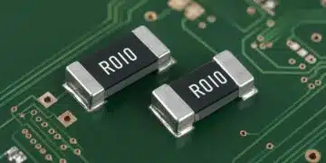
- Shunt and current‑sense resistors: These parts concentrate current and heat in small areas. Poor copper adhesion, insufficient copper thickness, or marginal via arrays in the current path can lead to hot spots, local delamination, and progressive resistance drift or intermittent opens.
- High‑capacitance MLCCs and large film capacitors: Large packages and high electro‑mechanical forces during thermal cycling or board flex place significant stress on solder pads. Thin solder mask dams, weak pad adhesion, and poorly balanced copper can accelerate pad lifting and crack formation at the component termination.
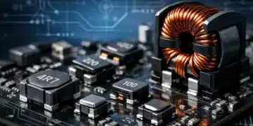
- Power inductors and transformers: Heavy magnetic components often sit on reinforced copper areas with multiple vias for current sharing. If via barrels are marginal or the board is unnecessarily thick, thermal cycling and vibration can induce barrel cracks that increase losses or cause intermittent failures under load.
- Connectors and terminals: Repeated mating cycles and cable forces transfer mechanical stress into pads and vias. Robust anchoring with adequate pad size, through‑hole stakes, or via‑in‑pad structures, combined with strong copper‑to‑laminate adhesion, is essential to avoid cracked solder joints and lifted pads.
A practical approach is to treat PCB reliability tests (such as IST, thermal cycling, and peel‑strength checks) and component derating as parts of the same system‑level qualification. Aligning board thickness, via concepts, pad designs, and material choices with the mechanical and thermal characteristics of key components greatly reduces the risk of “no trouble found” field returns and intermittent faults.
Conclusion
PCBs are far more than “green plates with copper.” They are the product of tightly controlled chemical and mechanical processes, a dense network of test and inspection steps, and a wealth of laboratory methods aimed at understanding and improving reliability. Inline monitoring, AOI, X‑ray alignment, electrical testing, microsections, and advanced techniques such as TMA, FTIR, XRF, climatic testing, and IST together form a comprehensive quality and reliability ecosystem.
For design and purchasing teams, the key implication is that PCB quality cannot be reduced to a few line items in a drawing or a lowest‑price quote. Decisions about design rules, copper balancing, stackup thickness, material selection, and required documentation have a direct impact on yield, time‑to‑market, and long‑term field performance. Engaging with the PCB manufacturer early, aligning on realistic tolerances and test plans, and leveraging available lab capabilities are essential steps to tap the full potential of “the underestimated PCB.”
By treating the PCB as a critical system component – with its own reliability engineering and qualification needs – organizations can significantly reduce risk, avoid late redesigns, and build more robust electronic products that perform reliably in demanding environments over many years.
FAQ: PCB Test Methods, Quality, and Reliability
PCBs are often treated as simple carriers for components, but they are complex engineered systems. Their reliability depends on controlled chemical processes, multilayer alignment, electrical testing, and long-term environmental validation. Poor PCB quality can compromise the entire electronic assembly.
The process starts with copper-clad FR-4 cores, continues with photoresist lamination, UV exposure, development, etching of inner layers, multilayer pressing with X-ray registration, drilling and plating, pattern plating and etching, solder mask application, final surface finish (e.g. ENIG), electrical test, routing, inspection and final packing.
Inline controls include monitoring chemistry concentration, pH, temperature, spray pressure, and dwell times in horizontal process lines. These parameters ensure stable etching, plating, cleaning, and resist development before formal quality gates are reached.
Key quality gates include inner-layer AOI, X-ray layer registration, electrical testing, impedance coupon measurement, and final AOI against a golden board. These steps catch defects that cannot be detected later in the process.
Inner-layer AOI uses high-resolution cameras and multi-color lighting to compare copper patterns against Gerber data, finding shorts, opens and geometry errors before lamination, with selectable coverage from sampling to 100% testing for safety-critical applications.
X‑ray registration is used to measure the position of buried inner‑layer targets after lamination so that drilling can be accurately aligned to all pads inside the multilayer. FR‑4 behaves like a composite during pressing, and resin flow, glass weave, and copper imbalance can cause complex shifts of inner layers. X‑ray systems detect these shifts and apply drill compensation, and panels outside the allowed registration window can be sorted out before drilling to avoid misaligned vias and reduced annular rings.
Flying-probe or fixture testers apply around 10 V and tens of milliamps for continuity with limits near 10 Ω, and verify isolation up to tens of megaohms or higher voltages on request, also checking 3D interconnects between different layers.
Microsections reveal internal structures such as copper thickness, dielectric layers, via barrel quality, and solder mask coverage. They are essential for first article inspection, failure analysis, and verifying compliance with IPC and customer-specific requirements. Microsection analysis removes small coupons from production boards, grinds and polishes cross-sections of vias and traces to measure copper thickness, dielectric thickness, solder mask coverage and via integrity, often including solder-shock tests to reveal hidden defects.
Typical reliability testing includes climatic storage (e.g. 40 °C/92 %RH or 85 °C/85 %RH) with insulation resistance measurement, thermal shock and thermal cycling, peel-strength tests, interconnect stress testing (IST) and high-speed loss measurements on dedicated coupons.
Manufacturers can issue a certificate of compliance, detailed inspection certificates with microsections and measurements, first article inspection reports for new series and extended custom reports that define additional checks and sampling plans.
Thinner multilayer PCBs experience lower z-axis expansion during thermal cycling, which significantly reduces barrel and microvia fatigue and can multiply the number of surviving cycles compared with thicker otherwise identical boards.
A good PCB drawing goes beyond outline dimensions and layer count. It should define the required IPC class, material type, final board thickness and copper weight, critical design rules, and any controlled‑impedance structures. In addition, it is useful to specify minimum annular rings, surface finish, required documentation (for example, FAI with microsections) and any special tests such as high‑potential or IST that are needed for your application.
How to qualify a new PCB supplier
Selecting a new PCB manufacturer should be based on more than price and delivery time. The questions below help you assess whether a potential supplier’s processes, test methods, and documentation capabilities match the reliability requirements of your applications.
- Clarify IPC classes and design limits
Ask which IPC classes the manufacturer routinely supports for multilayer boards and what their typical design limits are for line/space, via drill sizes, and annular rings. A capable supplier will state that they regularly build to IPC‑6012 Class 2 and Class 3, including HDI, and can quote realistic minimums such as 75–100 µm line/space for standard technology and 0.20–0.25 mm finished via drills, plus recommendations for more generous annular rings in high‑reliability designs. - Review inline process control and chemistry monitoring
Discuss which parameters are monitored inline on horizontal lines and how often they are verified by the in‑house lab. Look for continuous control of chemistry concentration, pH, temperature and spray pressure with trend charts, automatic dosing, defined alarm thresholds and regular lab cross‑checks (for example once per shift or daily) using titration and reference measurements. - Check AOI coverage, resolution, and reporting
Ask which AOI systems are used on inner and outer layers, what resolution they offer and what percentage of layers is inspected. For demanding products, you want inner‑layer AOI with around 25 µm resolution and configurable coverage up to 100 %, clear defect classification (shorts, opens, neck‑downs, contamination) and the ability to receive AOI statistics or sample images as part of the documentation. - Confirm X‑ray registration and drill compensation
Verify that multilayer panels pass through X‑ray registration after pressing and before drilling, and that drill programs are automatically compensated based on the measured inner‑layer target positions. A strong supplier blocks panels that fall outside the agreed registration window before drilling, preventing misaligned vias and reduced annular rings from reaching assembly. - Assess reliability testing capabilities
Ask which standard reliability tests are available in‑house and which are run with accredited partners. A robust portfolio includes climatic storage and CAF/SIR tests (e.g. 40 °C/92 %RH or 85 °C/85 %RH), thermal cycling with resistance monitoring, peel‑strength testing of copper adhesion and interconnect stress testing (IST) on tailored coupons, used both for qualification and process changes. - Define documentation level and FAI expectations
Clarify which documentation packages the manufacturer can provide for different risk levels: simple certificates of compliance for standard work, inspection certificates with microsections and dimensional data for important series, and full first article inspection (FAI) reports that must be approved before volume release. For critical programs, the supplier should be open to extended or customer‑specific reporting that includes chemistry logs, AOI statistics and relevant reliability test summaries. - Evaluate DFM and DFT support
Discuss how the manufacturer supports design‑for‑manufacturing (DFM) and design‑for‑test (DFT). The most valuable partners offer practical guidelines on stackups, via concepts, copper balancing and test‑point strategies, review critical layouts before release to fabrication and propose improvements based on experience. Regular technical reviews help align their process capabilities and test coverage with your reliability and cost targets.
How-to: Ensure High PCB Quality and Long-Term Reliability
- Choose appropriate materials and stack-up
Select base materials with suitable glass transition temperature, thermal expansion coefficients and dielectric properties, and design a balanced copper distribution across layers to minimize warpage and registration shifts during pressing. Optimize PCB thickness and via structures for your reliability needs, considering that thinner boards and microvia concepts can significantly improve thermal cycling robustness when properly processed.
- Prepare clean design data and realistic tolerances
Provide consistent Gerber or ODB++ data, drill files, stack-up tables and dimensioned drawings, avoiding unnecessarily tight gaps or mechanical tolerances where ample space is available, so that process windows remain robust. Clearly define critical tolerances such as controlled impedance, annular rings, V-cut locations and edge definitions and discuss them early with the PCB supplier to align measurement methods and acceptance criteria.
- Specify online process control and AOI expectations
Ensure your manufacturer uses modern horizontal lines with monitored chemistry concentration, temperature, pH and spray pressure, with documented control charts, alarms and clear actions when limits are exceeded. Agree on AOI coverage for inner and outer layers, including minimum feature sizes, sampling plans or 100% inspection for critical products and how potential defects and process adjustments will be reported back to you.
- Include X-ray and drilling control for multilayers
Request X-ray measurement of inner-layer targets after lamination so that drill programs can be compensated for layer shifts caused by resin flow, glass weave and copper imbalance. Require that panels with registration errors outside the defined window are identified and scrapped before drilling, especially for dense HDI and fine-pitch designs with small annular rings.
- Define electrical testing and impedance control
Specify 100% electrical test for continuity and isolation at suitable voltage and resistance limits, and add high-voltage testing if your application involves elevated operating or hipot levels. For high-speed or RF designs, require dedicated impedance coupons placed near your boards, along with target values, tolerances and final impedance reports for each production batch.
- Plan documentation, first article inspection and microsections
For new or critical projects, order a first article inspection that includes microsections of vias and differential pairs, copper and dielectric thickness measurements, solder mask coverage checks and dimensional verification. Agree on which measurements will be repeated during series production and which documents you will receive regularly, such as certificates of compliance, inspection reports and traceable lab results.
- Use laboratory analysis to validate materials and finishes
Ask your PCB partner how they use TMA, FTIR, peel strength testing and X-ray fluorescence to qualify incoming materials and to monitor the stability of solder masks, base laminates and metallic finishes over time. For high-reliability designs, consider requesting summarized lab data that confirms minimum peel strength levels, finish thicknesses and glass transition temperatures for each relevant material family in your project.
- Perform climatic and thermal cycling reliability tests
Define test vehicles or coupons with representative via structures and trace geometries and subject them to combined temperature and humidity tests, as well as thermal cycling profiles that mimic assembly reflow and field conditions. Monitor insulation resistance and interconnect resistance during these tests, then use microsections of failed coupons to identify root causes such as barrel cracks, pad lifting or inner-layer separations and feed the findings back into design and process improvements.
- Leverage interconnect stress testing for faster feedback
Where available, use interconnect stress testing on tailored coupons to accelerate thermal fatigue and obtain statistically meaningful cycle-to-failure data for different stack-ups, thicknesses and via concepts. Compare IST results for design variants to choose the most robust combination of layer count, board thickness and via technology for your reliability and cost targets.
- Continuously optimize design rules with your PCB supplier
Establish a feedback loop with your PCB manufacturer to review quality data, field returns and test results, adjusting design rules such as clearances, copper balancing and via structures to improve yield and robustness. Regular technical discussions and joint design reviews help ensure that process capabilities, test coverage and documentation evolve with your product roadmap and reliability expectations.