




Stephen Oxley, Business Development Engineer of TT Electronics, presents his best 10 strategies for incorporating High Voltage Resistors into designs, with a focus on prioritizing definition and testing of these integral components at the outset of the design process.
Key Takeaways
- High Voltage Resistors are critical in applications like defibrillators and medical X-rays.
- Select the right resistor technology based on voltage ranges, power capabilities, and specific application needs.
- Design for insulation coordination and standards, adhering to IEC requirements for creepage distances.
- Derate resistors for long-term reliability, typically operating at 50-70% of their rated values.
- Optimize PCB layout to enhance safety and performance in high-voltage designs.
“High voltage” is a term that can have several meanings, but here we are considering circuits with voltages from 1 to 100kV. An example from the lower end of this scale is an automatic external defibrillator, in which a capacitor is charged to up to 5kV before delivering a potentially life-saving, precisely calibrated electrical surge to a patient.
Staying with the healthcare theme but at the other end of the scale, we have medical X-rays, which are generated by accelerating electrons with around 70kV, then abruptly stopping them with a metallic target. Carefully controlled variation in this voltage allows the system to be adjusted to capture the image of soft tissue or different bone thicknesses.
These are just two examples of high-voltage applications in which resistors, usually the simplest of commodity components, are elevated in importance to provide critical protection and accurate control in demanding applications. This article presents ten tips based on support given over many years to designers needing high-voltage resistors, not just in medical, but also in industrial, transportation, and scientific sectors.
Resistor Technologies for High Voltage Applications
High‑voltage resistors are available in several construction types, each optimized for different combinations of maximum voltage, power, pulse behaviour and frequency range. Choosing an appropriate technology is just as important as calculating resistance values and voltage ratings.
As a starting point, designers typically consider metal glaze or metal oxide film resistors for general high‑voltage use, thick‑film chip resistors where compact size and automated assembly are important, and wirewound or bulk ceramic resistors where high energy, current limiting or special pulse requirements dominate. More specialized geometries, such as rod‑type or integrated voltage divider assemblies, are used when very high voltages, metrology‑grade accuracy or controlled electric field distributions are required.
The table below summarizes the main resistor families commonly used in high‑voltage circuits. It is intended as a technology overview; detailed selection guidance is available in the Resistor Technology Selection and Benchmark Guidelines and High Voltage Resistor Selection Guide articles on this blog.
| Technology | Typical voltage range | Power / pulse capability | Frequency / parasitics | Typical applications |
|---|---|---|---|---|
| Metal glaze / metal oxide film | From a few kilovolts up to tens of kilovolts per resistor, depending on body length, coating, and creepage distance. | Good continuous power handling with strong surge capability; well suited to lightning‑impulse and overload testing when correctly derated. | Moderate parasitic capacitance and low inductance; generally suitable up to the low‑MHz range for most control and measurement functions. | General high‑voltage dividers, bleeder networks, and current‑limiting elements in industrial and medical equipment. |
| High‑voltage thick‑film chip | Typically up to several kilovolts per resistor, limited by chip size and surface creepage; higher voltages achieved using series stacks or special designs. | Moderate power rating with good pulse capability when operated within manufacturer surge curves and thermal derating guidelines. | Very low inductance and relatively low capacitance; well suited to compact surface‑mount layouts and fast control loops in modern electronics. | Bias networks, compact divider chains, high‑voltage measurement in densely packed PCBs, and SMPS control circuitry. |
| Wirewound and power film | Typically limited to a few kilovolts per component, with extended capability possible using long bodies or dedicated insulation schemes. | Very high continuous power and pulse‑energy capability, making them ideal for current‑limiting, braking, and high‑energy surge applications. | Significant inductance due to the wound structure; best suited to mains‑frequency or low‑frequency applications, or where additional inductance is acceptable or even beneficial. | Current limiting, damping and snubber networks, and power resistors in drives and protection circuits. |
| Bulk ceramic / rod‑type | Designed for very high voltages, often in the tens of kilovolts range, using controlled surface fields and corona‑resistant geometries. | High average power dissipation and strong impulse performance when properly cooled and mechanically supported to manage thermal and mechanical stress. | Capacitance strongly dependent on geometry and environment; used where electric field control, partial discharge behaviour, and long‑term insulation stability are critical. | High‑voltage power supplies, X‑ray and accelerator equipment, laboratory dividers, and pulsed‑power systems requiring robust insulation and field control. |
| Integrated divider assemblies | Voltage ranges from a few kilovolts up to hundreds of kilovolts across multi‑resistor stacks, encapsulated modules, or oil‑immersed assemblies. | Power and pulse capability depend on the chosen resistor technologies and packaging; designs are typically optimized for specific metrology or converter feedback applications. | Frequency response defined by mechanical layout, shielding, and grading networks; can be tailored for DC metrology, low‑drift measurement, or wide‑band feedback and monitoring systems. | Precision voltage dividers, metrology‑grade measurement chains, and high‑voltage feedback networks in power converters and test equipment. |
Insulation Coordination and Standards
Insulation coordination for high‑voltage resistors and their surrounding PCB layout is governed by both component data sheet limits and system safety standards. For equipment connected to low‑voltage supply systems up to 1000 V AC or 1500 V DC, IEC 60664‑1 defines creepage distances, clearances and pollution degrees, and its latest editions and amendments refine these tables and test requirements. Designers should verify that the creepage and clearance distances around high‑voltage resistors meet or exceed the applicable IEC 60664‑1 requirements, taking altitude, pollution degree and material group into account.
In many audio‑video and ICT applications, IEC 62368‑1 has replaced legacy IEC 60065 and IEC 60950 safety standards, shifting the emphasis to hazard‑based safety engineering. High‑voltage resistors that form part of protective networks or that bridge isolation barriers must therefore be evaluated not only against limiting element voltage and surge ratings, but also with respect to their role in limiting accessible energy and maintaining insulation coordination under fault conditions. Older data sheets may still reference IEC 60065 impulse tests or similar legacy requirements, and these can be interpreted as component‑level robustness benchmarks within the broader IEC 62368‑1 framework adopted by modern equipment designs.
Design notes on derating and reliability
Although limiting element voltage and rated power provide clear upper limits, high‑voltage resistors should not be operated continuously at their maximum ratings in demanding applications. For long‑term stability and margin against manufacturing variation, it is good practice to design for continuous operating voltages and powers in the range of 50% to 70% of the rated values, and to validate performance with additional surge and overload tests representative of the end equipment.
Surge ratings specified for standard waveforms, such as 1.2/50 µs impulses or 10/700 µs telecommunication surges, are usually based on limited numbers of test pulses and specific duty cycles. When repeated surges or combined thermal and electrical stress are expected, resistors should be derated and tested under realistic conditions, including temperature cycling and humidity, to confirm that their drift and failure modes remain acceptable over the equipment life.
Potting compounds and oil immersion can significantly improve insulation coordination and surface tracking performance, but they also introduce the possibility of voids, contamination and partial discharge within the encapsulation. High‑voltage assemblies should therefore be verified at operating voltage for partial discharge, and designers should consider an additional derating margin to account for long‑term changes in the encapsulant and any manufacturing tolerances in the assembly process.
High‑Frequency and Fast Transient Behaviour
At higher frequencies and during fast voltage transitions, the behaviour of high‑voltage resistors is influenced by their parasitic capacitance and inductance, as well as by the surrounding layout and shielding. In voltage dividers used for measurement and control, the effective transfer function becomes frequency‑dependent, and small stray capacitances across series resistors can distort the divider ratio for fast edges and high‑frequency signals. These effects are more pronounced in long body, high‑voltage resistors and in stacked assemblies, and they must be considered whenever wide‑band measurement accuracy or fast transient reproduction is required.
For metrology‑grade high‑voltage dividers and precision feedback networks, designers often adopt coaxial or guarded mechanical arrangements, minimize loop areas and use shielded structures to control electric fields and leakage paths. Matching the parasitic capacitances of the divider elements and carefully routing return paths can significantly improve the high‑frequency response, while appropriate resistor technology selection (for example, low‑inductance thick‑film chips for compact, fast‑response circuits or optimized bulk ceramic assemblies for laboratory dividers) helps ensure that the inherent parasitics of the components align with the intended bandwidth and accuracy targets.
Ten Tips
1. Understanding voltage ratings
The primary voltage rating of a resistor is its limiting element voltage (LEV), sometimes called the working voltage. This is the maximum continuous voltage that may be applied across a resistor whose ohmic value is greater than or equal to the critical resistance.
Below this value, the maximum voltage is restricted by the power rating (Pr) to 2√Pr .R . Generally, it is DC or AC rms, but the datasheet for high voltage parts may define it as DC or AC peak.
Associated with this is the overload voltage rating, which is generally 2 or 2.5 times the LEV for 2 to 5 seconds. Often, much higher peak voltages can be withstood for short durations, as indicated in the pulse performance section of a datasheet. The final rating is the isolation voltage, which is the maximum continuous voltage that may be applied between the resistor and a conductor in contact with its insulated body.
2. Voltage division with discrete resistors
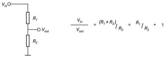
Voltage division requires a high-value resistor R1 in series with a low-value resistor R2 as shown in Figure 1. The voltage ratio is given by equation as shown in the Figure.
It should be noted that the voltage ratio is not the same as the resistance ratio R1 / R2 but is offset by one. For example, to obtain a voltage ratio of 1000, it is necessary to define a resistance ratio of 999. For a discrete resistor design, it is preferable to select standard values, and some examples for decade voltage ratios are presented in Table 1.
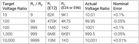
Having selected nominal values, the next consideration is the tolerance required. The tolerance in resistance ratio is simply the sum of the individual resistance tolerances. These are not necessarily the same; often it is most economical to select a tighter tolerance on the low-voltage part. For example, high voltage R1 at 1% and low voltage R2 at 0.1% results in a resistance ratio tolerance of 1.1%. For voltage ratios exceeding 50:1, the tolerance on the voltage ratio is effectively the same as that of the resistance ratio.
3. Specifying integrated voltage dividers
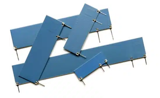
High-voltage dividers that integrate R1 and R2 into one three-terminal component are available, illustrated by TT Electronics’ HVD series (Figure 2). There are a number of precision advantages to this approach. For example, the target voltage ratio may be defined precisely, without the constraint of choosing standard values.
The values specified for integrated dividers are normally the low value R2 and the total value R1 + R2. Also, the tolerance on the voltage ratio can be controlled directly by the trimming process and so can be made considerably tighter than the absolute tolerances on the resistor values.
For example, R1 and R2 can be defined with 2% absolute tolerances, but the voltage ratio may be adjusted to a 0.5% tolerance.A similar advantage can apply in relation to the temperature coefficient of resistance (TCR), with the tracking TCR, which determines the temperature stability of the voltage ratio, being potentially lower than the absolute TCR of the resistor elements. Further, it is possible to design dividers that extend this element of matching to the areas of life drift and voltage coefficient of resistance (VCR), although this will typically call for a customised design.
4. Evaluating TCR and VCR errors in dividers
Provided the R1 value is sufficiently high, and the voltage sufficiently low, there will be a low level of self-heating in the divider. If this is the case, it is relatively easy to measure the TCR and VCR effects separately. Temperature coefficient of voltage ratio TCR effects are calculated using a temperature chamber, and the resulting figure of merit is defined as:

The corresponding figure of merit for Voltage Coefficient of Voltage Ratio VCR effects is similarly defined as:

in ppm/°C, where
- VRht and VRlt are the voltage ratios at high and low temperatures
- HT and LT are the high and low temperatures.
in ppm/°V
If self-heating is not negligible, then in the TCR test, the chamber temperature should be adjusted to give the correct HT figure, and time should be allotted for the temperature to stabilise. The VCR test should be short in duration to minimise temperature rise. Alternatively, one can use a temperature chamber to measure low voltages at higher temperatures and vice versa, thereby cancelling out temperature-related resistance changes.
5. Calculating the value of a bleed resistor
Bleed resistors are used to discharge capacitors to safe voltage levels after power is removed. A bleed resistor may be either switched across the capacitor for rapid discharge without quiescent dissipation, or permanently connected for high reliability and low cost.
In the latter case, there is a trade-off between the time to reach safe discharge and the quiescent power loss. Selecting a maximum suitable ohmic value is achieved from an exponential discharge calculation:

, where
- Td is discharge time
- C is capacitance value assuming maximum positive tolerance
- Vt is the safety threshold voltage
- Vo is the initial voltage
The highest standard value, which, allowing for tolerance, lies below Rmax should be used.
For a selected value R, the initial power is given Po = Vo 2/R . For a switched bleeder, this is the peak power. For a permanently connected bleeder, it is the continuous dissipation, and the resistor chosen must be rated accordingly.
Example: Consider a high‑voltage capacitor charged to 5 kV that must discharge to 50 V within 10 seconds after switch‑off, with a capacitance of 10 µF. Using the exponential discharge relationship, the required bleed resistance is
Where is the capacitance, the allowed discharge time, the initial voltage, and the target safety threshold voltage.
which yields a resistance in the tens of kilohms range for this combination of voltage, capacitance and time. Designers must then check that the continuous power dissipation at 5 kV is within the resistor’s rating and, if necessary, adjust the target discharge time or use multiple resistors to share the load.
6. Selecting the right balancing resistor
All aluminium electrolytic capacitors exhibit a leakage current when a DC voltage is connected across them.
This may be modelled by a leakage resistance connected in parallel with the capacitor. This resistance is non-linear, that is, its value is a function of the applied voltage. In this case, the value is poorly defined, having a large degree of variation from one capacitor to another.
When building a capacitive reservoir for a high-voltage DC bus, it may be necessary to use a series combination of two capacitors, each rated at half the bus voltage. If the capacitors are identical, the bus voltage will be shared equally between them.
However, in practice, the leakage resistances will differ, leading to uneven sharing and possible voltage overload on the capacitor with the higher leakage resistance.
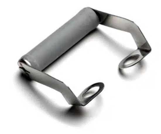
The solution is to use balancing resistors, such as that shown in Figure 3, in parallel with each capacitor. These are high-value resistors rated at the appropriate voltage and matched in value to within a few percent. The value needs to be as high as possible to minimise power dissipation, but is generally chosen so that it is no more than 10% of the lowest value of leakage resistance at the rated voltage of the capacitor. By this means, the effect of the unbalanced internal capacitor leakage resistance is swamped by that of the balancing resistors, and the voltages are approximately equalised.
Example: A simple 900 V DC bus can be built from two 450 V electrolytic capacitors in series. If the leakage current of each capacitor varies between 2 µA and 10 µA at operating voltage, selecting balancing resistors such that the balancing currents are at least an order of magnitude higher than the minimum leakage (for example, 50 µA or more) helps ensure that voltage sharing is dominated by the resistors rather than by the leakage variation. This corresponds to balancing resistor values in the tens of megohms range, and the resulting power dissipation must be checked against the resistor ratings and the overall efficiency budget.
7. Withstanding high voltage surges
It is sometimes the case that designers looking at high-voltage resistors are doing so because their circuit must withstand highvoltage transients. If the continuous voltage stress does not call for a high-voltage rating, it may well be the case that a low-voltage but surge-tolerant part is the best solution. For example, TT Electronics’ 5W wirewound high surge resistor, WH5S, does not have a high-voltage rating but can withstand a 1.2/50μs up to 10kV peak, whilst the surge tolerant 2512 chip resistor, HDSC2512, has an LEV of 500V but can withstand a peak voltage of up to 7kV.
8. Designing to meet safety standards
When designing equipment to meet the requirements of electrical safety standards such as IEC 60664, it is necessary at an early stage to consider the relevant creepage and clearance requirements.

These will not only affect PCB layout design but also, in some cases, component selection. Where a resistor connects to a high-voltage level, it is important to check the distance between its terminations, and, in the case of heatsink mounted parts, between the resistor and a metallic thermal interface. This is defined in two ways. Firstly, the creepage is the shortest distance across an insulating surface.
This reduces the likelihood of humid and contaminating conditions enabling surface scintillations with energy high enough to entail tracking. Secondly, the clearance is the shortest distance in air. This addresses the risk of flashover. These two dimensions, if not apparent from datasheets, should be available from the manufacturer. Another piece of information that may be needed is the material forming the insulating surfaces, as this determines the comparative tracking index (CTI), which classifies an organic material’s pro-pensity to support processes leading to tracking.
If a resistor bridges the isolation barrier in a design, for example, to provide a galvanic connection to prevent excessive electrostatic charge build-up, the IEC 60065 safety standard requires resistors to withstand a specified high-voltage surge test. As this is becoming a legacy standard, ongoing certification of resistors is no longer relevant. Still, designers following the hazard-based safety engineering approach of IEC 62368-1 will be helped in knowing that there are still products that meet the requirements of IEC 60065.
9. Optimising the PCB layout
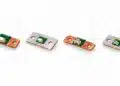
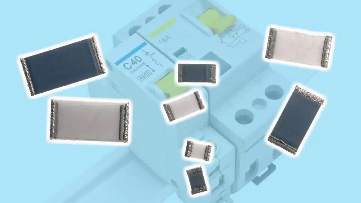
PCB layout is crucial to maintaining the safety of a high-voltage design, and this is most obvious where high-voltage resistors are miniaturised and in surface mount device (SMD) form. A good example is TT Electronics’ HVC series which includes a 2512 size chip resistor with a 3kV rating.
Tracks or vias beneath or very close to the component should be avoided, as should any features likely to trap or encourage ionic contamination during manufacture or use. One special measure which may be used to increase creepage distance and avoid trapped contamination is the cutting of a slot in the PCB beneath the component.
10. Designing for potted and oil-filled assemblies
Two limiting factors in high voltage designs can be the tendency of contaminated organic surfaces to support tracking and the risk of electrical discharge in the air, particularly around small radius surfaces. Both of these constraints can be tackled by potting or immersion in mineral oil, which prevents the ingress of contamination and replaces air with a substance of higher dielectric strength.
This in turn reduces creepage and clearance constraints allowing an assembly to be reduced in size. When choosing resistors for such an assembly, it is essential to select parts that are insulated in a manner that avoids the risk of outgassing. Any air incorporated with the component can form a void in which partial discharges can occur, leading to the long-term degradation of insulating materials.
This rules out the use of parts with insulation sleeving or with rough or porous coating finishes. An epoxy coating, either printed or powder dipped, is often ideal, and a manufacturer can advise on suitability.
High‑Voltage Resistor Selection Checklist
The design tips above focus on how to calculate stresses and select appropriate ratings. To complete a robust, vendor‑neutral selection process, it is useful to apply a systematic checklist that aligns electrical, environmental and mechanical constraints with a suitable resistor technology and package. The following steps summarize a practical approach that complements the Resistor Technology Selection and Benchmark Guidelines and the High Voltage Resistor Selection Guide published on this blog.
- Bound the operating stresses by defining continuous and worst‑case voltages, currents, power, surge energies, duty cycles and operating temperature ranges.
- Eliminate unsuitable technologies by checking basic limits such as maximum working voltage, surface load capability, inductance and frequency response, and known incompatibilities with the application environment.
- Select candidate resistor technologies and packages that can safely survive all electrical and environmental constraints, including pollution degree, altitude, humidity and contamination risk.
- Refine the choice based on required accuracy, stability and noise, considering tolerance, TCR, VCR, long‑term drift and pulse behaviour against the circuit’s precision and lifetime targets.
- Validate the selection with appropriate tests, such as surge and overload pulses, temperature cycling, humidity exposure and partial discharge checks for potted or oil‑filled assemblies, and document all derating and margin assumptions for future design updates.
Example of manufacturers available series and specification range
| Manufacturer | Series | Type | Resistance Range | Power Rating | Tolerance | Max Voltage | Temp Coefficient | Package / Style | Notes |
|---|---|---|---|---|---|---|---|---|---|
| Vishay | HVR Series | High-voltage film | 1 kΩ – 1 GΩ | 1 W – 10 W | ±1%, ±5% | up to 30 kV | 50 ppm/°C | Axial leaded | Designed for HV dividers |
| Ohmite | HVF Series | Thick-film | 10 kΩ – 100 MΩ | 1 W – 5 W | ±5%, ±10% | up to 20 kV | 100 ppm/°C | Axial / radial | For pulse applications |
| Caddock | MX480 Series | Film, precision | 100 kΩ – 1 GΩ | 2 W – 12 W | ±0.5%, ±1% | up to 40 kV | 25 ppm/°C | Custom modules | Precision HV networks |
| KOA | HV Series | Thick-film | 10 kΩ – 10 MΩ | 0.5 W – 3 W | ±1%, ±5% | up to 10 kV | 100 ppm/°C | Axial | General HV usage |
| TDK | Custom HV | Thick-film array | 1 kΩ – 100 MΩ | 0.25 W – 2 W | ±1%, ±2% | up to 15 kV | 50–100 ppm/°C | SIP/DIP networks | Integrated resistor nets |
| TT Electronics | HVD / HVC / F Series | Thick-film / divider | 25 kΩ – 150 GΩ | 0.3 W – 1.3 W | ±0.5% – ±10% | up to 3 kV (chips), up to 28 kV in oil, up to 30 kV for dividers | ±50 – ±100 ppm/°C (chips), tracking down to 25 ppm/°C for dividers | Chip SMD, planar, axial and encapsulated divider modules | Lead-free GHVC high-voltage chips, HVC/HVP planar resistors, and HVD precision divider assemblies for sensing and feedback. |
Conclusion
- In many cases, resistors can be regarded as the simplest of components in a circuit and need no special attention from designers beyond selecting an appropriate ohmic value and power rating.
- However, high-voltage circuits often call for a specialist component from a manufacturer who can provide experience and expertise.
- The designer is well advised to prioritise these as critical components for definition and testing at an early stage in the project, and to check whether a custom or semi-custom approach can add significant value.
High Voltage Resistors: FAQ
High voltage circuits are defined as operating from about 1 kV up to 100 kV, including applications such as defibrillators and medical X‑ray systems.
Voltage ratings such as limiting element voltage (LEV), overload voltage, and isolation voltage define the maximum continuous and transient voltages a resistor can safely withstand without breakdown.
Discrete resistor dividers are suitable when standard values and moderate precision are acceptable, while integrated dividers are preferred when you need a tightly controlled voltage ratio, better TCR/VCR tracking, and improved long‑term stability.
The temperature coefficient of resistance (TCR) and voltage coefficient of resistance (VCR) cause the divider ratio to drift with temperature and applied voltage, so designers must evaluate these coefficients to ensure accurate measurement and control over operating conditions.
Bleed resistors safely discharge capacitors to a defined threshold voltage after power is removed, balancing discharge time against continuous power dissipation using exponential discharge calculations.
Balancing resistors compensate for mismatched, non‑linear leakage currents in series capacitors, ensuring that each capacitor shares the DC bus voltage more evenly and avoids overvoltage stress.
If continuous voltage is modest but transient surges are high, surge‑tolerant resistors with suitable pulse ratings can be used instead of dedicated high voltage resistors.
Creepage (surface distance) and clearance (air distance) around resistor terminations and heatsinks must satisfy IEC safety standards to prevent tracking and flashover, which can influence both PCB layout and the choice of resistor package.
Good practice includes avoiding tracks and vias beneath SMD high voltage resistors, eliminating contamination traps, and, where necessary, adding PCB slots to increase creepage distance.
Potting or mineral oil immersion raises dielectric strength and reduces tracking and discharge in air, allowing more compact designs, provided that resistors use non‑porous, non‑outgassing insulation such as suitable epoxy coatings.
How to Design with High Voltage Resistors
- Step 1: Define your high voltage application and operating range
Start by specifying the DC or AC voltage range, from around 1 kV up to tens of kilovolts, including normal and worst‑case operating conditions.
- Step 2: Select resistors with appropriate voltage ratings
Choose resistors based on limiting element voltage (LEV), overload voltage, and isolation voltage to ensure safe continuous operation and transient handling.
- Step 3: Decide between discrete and integrated voltage dividers
Use discrete R1 and R2 when standard values and simpler designs suffice, or choose integrated dividers when you need a precise, trimmed voltage ratio and matched characteristics.
- Step 4: Evaluate TCR and VCR for accuracy
Assess temperature coefficient of voltage ratio and voltage coefficient of voltage ratio using controlled temperature and voltage tests so that the divider maintains accuracy over its full operating envelope.
- Step 5: Calculate bleed resistors for energy discharge
Determine bleed resistor values using exponential discharge equations to reach a safe voltage within the desired time while keeping continuous power loss within the resistor’s rating.
- Step 6: Specify balancing resistors for series capacitors
For high voltage DC buses using capacitors in series, select high value, well‑matched balancing resistors sized so that their resistance is typically no more than about 10% of the lowest leakage resistance.
- Step 7: Address surge and transient requirements
Identify surge waveforms and peak voltages, then select surge‑tolerant resistors whose pulse ratings and waveforms, such as 1.2/50 µs impulses, meet or exceed those stresses.
- Step 8: Design for safety standards and insulation
Apply IEC creepage and clearance rules, check component dimensions and CTI of insulating materials, and ensure that any resistor bridging isolation barriers satisfies relevant surge test requirements.
- Step 9: Optimize PCB layout for high voltage
Lay out the PCB to maximize creepage and clearance around high voltage resistors, avoid copper beneath SMD parts, and consider using board slots where necessary to control surface tracking paths.
- Step 10: Choose resistors suitable for potting or oil immersion
For potted or oil‑filled assemblies, specify resistors with smooth, non‑porous epoxy coatings and no trapped air so that void‑related partial discharges and insulation degradation are avoided.