


The contact interface, D in Figure 1.3 is arguably the heart of a connector system. The structure and properties of the interface which is created as the plug and receptacle contact springs come together determines both the electrical and mechanical performance characteristics of a connector.
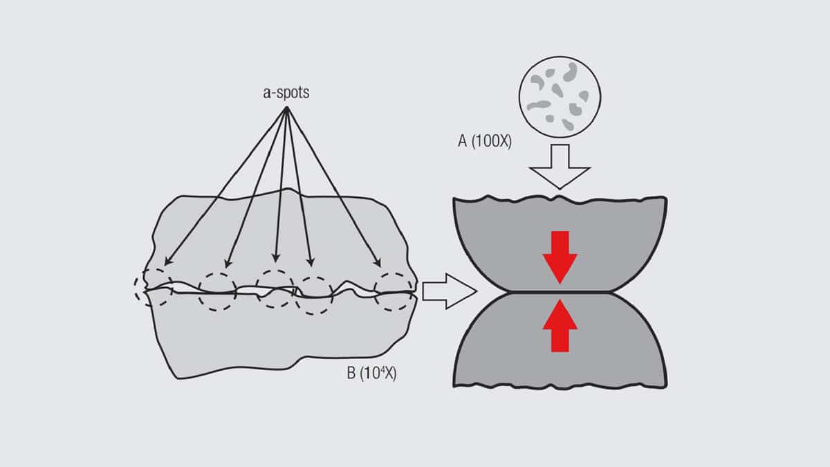
The most important characteristic of the contact interface is that it is created when two rough surfaces come into contact. While a cursory look at the surfaces of contact springs suggests that they are smooth, on the microscale of the contact interface these surfaces are quite rough. The individual high points on the surface are referred to as asperities. Figure 1.15 schematically illustrates the contact interface that would be created if two spheres were brought in contact under an applied load. As the two surfaces approach each other the asperities that happen to be in proximity to each other come together first. As these asperities deform against each other under the applied load, the surfaces continue to approach each other bringing additional asperities into contact. Thus, a contact interface consists of a number of individual asperity contact points, called a-spots. The number is determined by the roughness of the surface and the applied load which determines the total area of a-spot contact. These a-spots are distributed over an apparent contact area that is determined by the geometries of the post and receptacle contact springs as they come together.
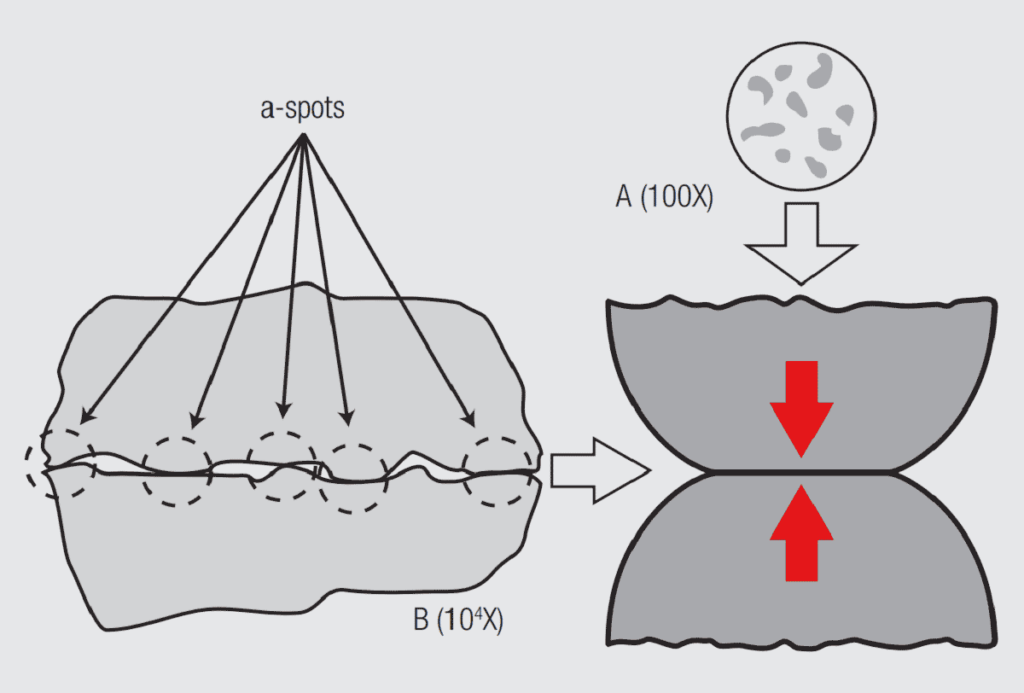
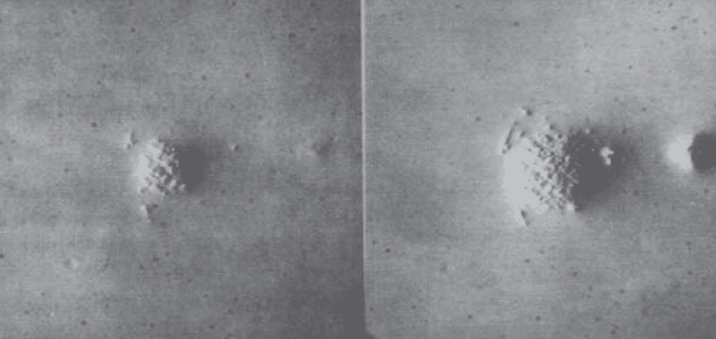
That this a-spot model is realistic is verified by consideration of Figure 1.16 which shows an actual contact interface between a stainless steel ball bearing and a glass plate. The ball bearing deforms slightly against the glass plate under the applied load and individual a-spots are created. Note the similarity to Figure 1.15. The photo on the right was taken after an increase in the applied load which brings the surfaces closer together. This, in turn, increases the contact area of existing a-spots as well as creating additional a-spots.
Returning to Figure 1.15, a side view of the contact interface, also shows a distribution of a-spots across the contact interface. This view will lead to an understanding of why the contact interface structure affects both the mechanical and electrical performance. Consider two mechanical effects. First, if a shear stress is applied to this a-spot contact interface the interface will remain stable until the stress is sufficient to break the a-spot interfaces. Second, when the interface does break a wear process comes into play. These two effects will be discussed in Chapter I/1.3.2 The Mechanical Interface: Friction and Wear/Durability.
Electrical performance is affected by the fact that any current flow from the upper sphere to the lower, would have to flow through the individual a-spots. This condition leads to an electrical resistance called constriction resistance which will be discussed in some detail in Chapter I/1.3.3 The Electrical Interface: Contact Resistance.
The Mechanical Interface: Friction and Wear/Durability
Friction and wear are two aspects of the same basic kinetic process. Friction forces must be overcome to cause motion, and motion must occur to cause wear. Consideration of Figure 1.17 will be used to explain this statement.
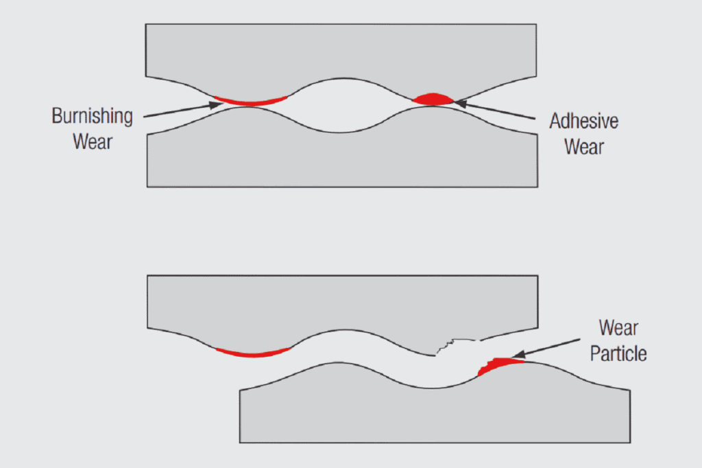
Consider Figure 1.17 through a thought experiment where two a-spot contacts are created. The a-spot on the right is created first under a given applied load. The individual asperities deform against each other under the load. Four things happen during the deformation. First, the asperities deform plastically due to their small size causing material flow. Surface films and contaminants are disrupted or displaced on the microscale of the flow. Second, the clean metal surfaces exposed due to the microflow can form cold welded junctions when the microflow ceases. Third, the asperity surfaces work harden due to the deformation. Fourth, the a-spot contact area increases as the load increases.
While all this is happening at the first asperity contact the surfaces are continuing to come closer to one another and the second a-spot is created. The same process then begins to take place at this second a-spot. We now have two a-spots that have experienced different amounts of deformation. The difference in deformation means that the first a-spot is larger, due to more metal flow, and stronger – due to a greater work hardening response and more cold welding.
The increased area and strength of the first a-spot means that it will be mechanically more robust. Consider how the two a-spots will respond under an applied shear stress. This discussion is qualitative and only serves to illustrate the kinetics of friction and wear.
The applied shear stress will not lead to motion of the interface until the a-spots are broken. Given that the first a-spot is larger and stronger, it will determine the stress necessary to break the interface and cause motion. The necessary stress is related to he friction force of the contact interface. Thus the a-spot structure and distribution determines the friction force and, therefore, the mechanical stability of the contact interface.
The kinetics of separation at the a-spot interfaces will be different as well. Recall that the interface of the first a-spot is stronger than that of the second. In fact, due to work hardening and cold welding, the interface may be even stronger than the cohesive strength of the base metal. In such cases, the a-spot interface may break within the base metal rather than at the interface resulting in a wear particle as indicated in Figure 1.17. Such wear processes are commonly referred to as adhesive wear. In contrast, the weaker interface of the second a-spot may break at or near the original interface without a wear particle being generated. Wear of this type is referred to as burnishing wear. The wear track in a connector experiencing adhesive wear, sometimes called galling wear, will be rough, while that of burnishing wear will be relatively smooth.
The significance of wear processes in a connector is straightforward. Wear results in the loss of surface material. If a connector is designed to take advantage of the benefits of a contact finish, wear can lead to loss of the contact finish at the mating area and a consequent decrease in performance. This is particularly significant when the small thicknesses of contact finishes are recognized. Susceptibility to wear is one reason connectors are rated for a specific number of mating cycles.
Friction has two effects on connector performance, one positive and one negative. The positive effect is that friction provides mechanical stability of the contact interface against forces tending to drive motion of the connector. Disturbances of the contact interface can be a significant degradation mechanism for a connector for two reasons. First, the micromotions of a contact disturbance can induce wear at the contact interface. Second, micromotions can drive corrosion mechanisms, especially in tin finished contacts, and can lead to bring corrosion products and contaminants around the contact area into the contact interface. Thus high friction forces, generally due to high contact normal forces, can have a positive effect on connector performance.
There are two negative effects of friction forces. First, high friction forces correlate directly with wear mechanisms as has been discussed. Second, high coefficients of friction will increase the mating force of a connector. Mating force varies directly with the coefficient of friction.
These issues, friction, mating force, contact force and wear will be discussed in detail in Chapter II/2.2.1 Separable Interface Requirements.
The Electrical Interface: Contact Resistance
Attention now turns to the effects of a-spots on electrical performance, and, in particular on the electrical resistance the contact interface introduces into the connector. Toaddress that issue requires a discussion of the sources of resistance in a connector.
Figure 1.18 shows a cross section of a connector with the various sources of resistance indicated. There are three types of resistances noted. There are two permanent connection resistances RP.C., the resistance of the crimped connection to the incoming conductor and of the pin connection to the plated through hole of the printed circuit board. Permanent connection resistances are dependent on the permanent connection technology used. There are also two bulk resistance contributions RB, from the pin and receptacle contacts individually. Bulk resistances are determined by the resistivity of the material of the contact spring and its geometry. Finally, there is the resistance of the contact interface RC. Only one resistance is cited even though there are two contact interfaces electrically in parallel.
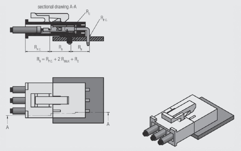
In order to get a perspective on the relative contributions of these three resistances, consider the following thought experiment. If a test probe is inserted through the insulation to the conductor of the wire coming into the crimped connection and a corresponding probe placed in contact with the pad on the plated through hole connection the overall resistance Roverall of the connector can be measured. To provide a benchmark, it is assumed that the connector system shown uses a 0.64 mm (0.025 in) square post. For a connector of this size a reasonable value for the overall resistance is of the order of 20 milliohms. The permanent connections will be less than a milliohm each, the bulk resistances will total about 17 milliohms and the contact resistance will be of the order of a milliohm. Thus, for this connector system the contact interface resistance is of the order of five percent of the overall resistance. Why then is the contact interface resistance so important? The answer is found when the connector system is subjected to a test program to assess its stability under a variety of conditions. If, after such testing, the overall resistance of the connector is measured and found to be, say, 200 milliohms virtually all that change will be in the contact interface resistance.
Bulk resistances are essentially constant. Permanent connection resistances tend to be stable because they have larger contact areas and contact forces than separable interfaces. So, an understanding of the parameters that determine contact interface resistance is critical to knowing how to design and maintain its integrity over the broad range of connector applications and application environments.
As noted previously, electron flow can only occur through an a-spot, the majority of the apparent contact area is non-conductive. This means that the current distribution through the contacts is constricted to pass through individual a-spots at the contact interface. This geometrical current constriction gives rise to constriction resistance as illustrated in Figure 1.19.
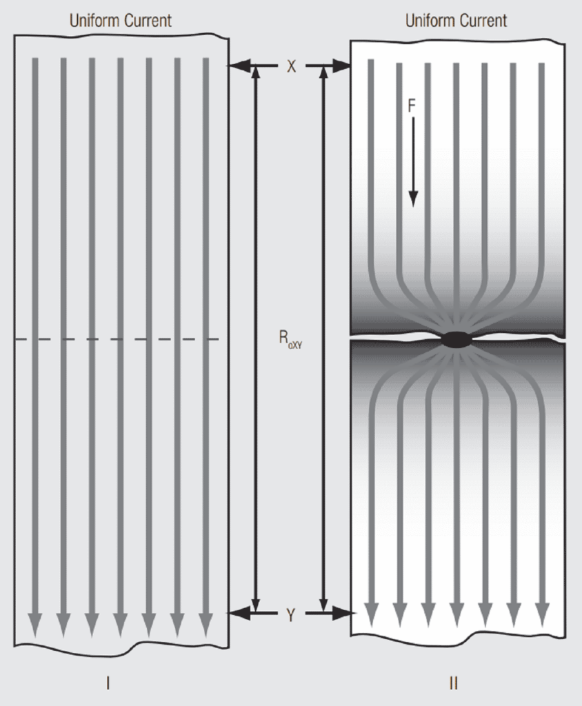
Another thought experiment. The drawing on the left in Figure 1.19 depicts a length of round conductor. Voltage and current probes are connected to the conductor at points X and Y so that a direct current voltage can be applied between points X and Y and the resulting current measured. Ohm’s law, V = I R, where V is the voltage drop, I is the current and R the resistance, can be used to calculate the resistance.
An additional, independent, way to calculate the resistance is using the below relationship: where r is the resistivity of the conductor material, L the length between X and Y and A is the cross sectional area of the conductor. Naturally, these two methods result in the same value of resistance.

Now for the thought part. Assume that a zero thickness blade can be used to cut into the conductor midway between X and Y down to an infinitesimal distance from the center of the conductor. Given that change in conductor configuration the resistance is once again calculated using Ohm’s law. The new calculated value will be much higher than the original value. To explain why we can use our general formula R = r (L/A).
In the original conductor in Figure 1.19 the DC current is indicated by a uniform distribution of current flow lines across the conductor cross section. This, of course, is not what actually happens, but serves as a good visual representation for this discussion. The flow lines are all the same length and distributed uniformly over the conductor cross section.
In the reduced cross section conductor a very different flow pattern exists. If the cut to the center is small enough only one of the flow lines can pass along the conductor unimpeded. All the other flow lines must constrict to flow through the single continuous thread of conductor. This is the source of the term constriction resistance to describe this effect.
Now consider the general formula. Recall that the length of all the flow lines but the central one must increase in length in the new configuration. R is directly proportional to L in the general formula which explains the increase in resistance. Alternatively, note that the current flow lines begin to constrict at some distance away from the reduced cross section. This effect can be modeled by taking a number of slices perpendicular to the axis of the conductor and noting that the cross sectional area of each currentcarrying slice is smaller than the original cross section. R is inversely proportional to A so each of these slices has a higher resistance then the original slice, and all these slices are in series, thus, the increase in resistance.
Note that there is no interface in this model, the conductor is continuous. Constriction resistance is a geometric effect. All contact interfaces will include a number of a-spot interfaces, each of which will introduce a constriction resistance. Thus an interface must produce an increase in resistance to the connector. This resistance can be minimized by maximizing the a-spot contact area, but it cannot be eliminated.
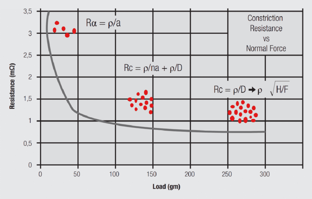
The resistance in Figure 1.20 is the constriction resistance, the resistance of the metal-to-metal contact interfaces. As the plug and receptacle surfaces are brought together under the contact normal force, a few asperity contact interfaces form, as illustrated previously in Figure 1.15, such contacts are referred to as a-spots. The resistance of each individual a-spot, Ra, is given by the formula shown in Figure 1.20:

where ρ is the resistivity of the material, and ad is the diameter of the a-spot. As the force is increased and the surfaces deform against one another additional a-spots are created. The second equation now applies:

Where Rc is the contact interface resistance, n is the number of a-spots in parallel and D is the diameter of the apparent contact area, the area over which the a-spots are distributed at the contact interface. These two resistances are in series because the current constricts first to the dimensions of the apparent contact area, defined by D, and then constricts again to flow through the individual a-spots, defined by ad.
As the contact force continues to increase, the number of a-spots increases along with the apparent contact area. As n increases the a-spot resistance contribution decreases and the contact interface resistance becomes dominated by the resistance due to the apparent contact area. In other words, the interface acts like a single contact area with a diameter determined by the contact geometry.
At this point, the contact resistance can be calculated by the final formula:

where H is the hardness of the contact material and F the contact force. The units of hardness are force/area so the square root of the inverse of hardness gives the diameter of the contact area. This equation shows why the contact force is a fundamental parameter of connector design.
The distribution and number of a-spots provides a highly redundant network of resistances in parallel at the contact interface, a very important factor in the stability of contact interface resistance. It must be noted that permanent connection interfaces are also created in the same manner, and differ only in the amount of deformation, cold welding and the total contact area that is created.
A summary of the effects of the a-spot surface structure of contact interfaces follows:
• On the microscale of the contact interface all surfaces are rough.
• Surface roughness leads to the creation of small individual contact areas, called a-spots, at the contact interface.
• The number of a-spots created depends on two factors: the contact force and the surface roughness. The contact force determines the total a-spot contact area and the surface roughness determines how many a-spots will be included in that area.
• The geometry of the apparent contact area containing the a-spots is determined by the geometries of the plug and receptacle contact surfaces as they come together during mating.
• Current flow across the contact interface is constricted to flow through the a-spot distribution a geometric effect leading to an increase in resistance, constriction resistance, at the contact interface.