


In this Würth Elektronik webinar you will learn more about PCB design rules and layout.
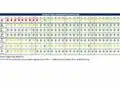
Würth Elektronik BASIC Design Rules have been revised and restructured. Did you know, for example, that for PCB manufacturing processes, the parameter “conductor width” is quite insignificant? The webinar is interesting for purchasing, developers and students.
- BASIC and standard – what is the difference?
- BASIC Design Rules – the current status
- IPC compliant copper thicknesses
- Current solder mask parameters
Basic Design Rules for PCB Layout According to World Electronic Parameters
This presentation provides a comprehensive overview of the fundamental design rules and layout principles for printed circuit boards (PCBs), focusing on evolving practices influenced by world electronic parameters. It highlights key updates, technological advancements, and best practices for efficient PCB design, ensuring high-quality manufacturing and reliability.
Introduction
The evolution of PCB design rules over the past decade reflects significant advancements in electronic circuit board technology. This document outlines the updated basic design rules, originally presented in 2013, with a focus on their relevance to contemporary PCB technologies like HDI micro-via, embedding technology, and flex solutions.
1. Basic vs. Standard: Defining the Concepts
- Standard: A classification system applicable across technologies, including standard stack-ups and delivery specifications that ensure quality, cost-effectiveness, and quick turnaround times.
- Basic Technology: Refers to the foundational PCB types—single-sided, double-sided, and multi-layer boards. It encompasses standard and advanced classifications within its scope.
2. Scope of Application
The updated basic design rules apply universally across PCB technologies, including:
- Copper structures and spacings
- Drills, drill pads, annular rings
- Edge plating, solder masks, peelable masking
- Markings and delivery specifications
3. Key Updates and Changes
- Copper Structuring: Enhanced rules for both inner and outer layers, detailing positive imaging, subtractive etching, and selective copper deposition processes.
- Specification of Copper Thickness: Alignment with IPC standards to ensure consistency in manufacturing.
- Aspect Ratio for Drill Holes: New guidelines to maintain structural integrity and metallization quality.
4. Design Rules in Detail
- Conductor Spacing vs. Width: Emphasis on the critical role of conductor spacing in manufacturing reliability.
- Annular Rings: Necessary for both through-hole technology and electrical connectivity to maintain registration tolerance.
- Aspect Ratio: Defined as the ratio of drill diameter to PCB thickness, impacting metallization and drill pad requirements.
5. Practical Application Example
A case study on flex-rigid boards with HDI technologies illustrates the application of new design rules, emphasizing:
- Optimized line widths and spacings
- Enhanced solder mask coverage
- Improved yield and production efficiency
6. Poll Results and Feedback
Insights from interactive polls reveal user preferences and areas for further improvement in the design rules document:
- High user satisfaction with updated rules
- Areas identified for potential optimizations
7. Summary and Conclusions
- Basic technology covers key PCB types, while standards serve as classifications for design and manufacturing.
- Conductor spacing significantly influences manufacturability.
- Annular rings and aspect ratios are vital for structural integrity.
- Continuous feedback helps refine design rules for evolving technologies.