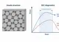


This article and Würth Elektronik webinar examines the fundamental principles of EMC filter design, from component-level characteristics through complete system integration, providing engineers with actionable insights for conducted emission mitigation in power electronics and communication systems.
Key Takeaways
- This article explores EMC Filters Explained, focusing on design principles, component selection, and integration challenges.
- It highlights the importance of understanding interference mechanisms, frequency-dependent parameters, and component behavior.
- The article discusses various filter topologies, their effectiveness, and common filtering issues to avoid.
- Practical design examples, such as RS-485 filtering, demonstrate real-world applications and simulation validation.
- Key takeaways emphasize the need for careful component choice, layout optimization, and validation processes in filter design.
The presentation deal with the following topics:
- The need for filters and different topologies
- Components and technologies
- Choosing components for a filter
- Design and simulation of filters
- How to destroy a filter
EMC Filters: From Component Selection to Practical Design
Electromagnetic compatibility (EMC) filter design requires systematic understanding of component behavior, filter topology, and practical implementation challenges.
1. Introduction
Electromagnetic interference (EMI) represents one of the most persistent challenges in modern electronic system design. As switching frequencies increase and circuit densities rise, conducted emissions from DC-DC converters, AC-DC power supplies, and high-speed digital circuits frequently exceed regulatory limits set by standards such as CISPR 22 and EN 55032
EMC filters are not merely collections of passive components enclosed in potting material; they are sophisticated frequency-selective networks whose performance depends critically on component selection, placement, and understanding of parasitic effects. A well-designed filter addresses both common-mode and differential-mode interference while maintaining signal integrity and meeting safety requirements.
This white paper presents a comprehensive approach to EMC filter design, drawing from practical engineering experience and measurement data to illustrate key principles. We examine why filters fail in real applications, how to select appropriate components based on frequency-dependent parameters, and proven techniques for optimizing filter performance.
Modern EMC Challenges and Design Trends
Contemporary electronic systems face evolving EMC challenges driven by technological advancement and miniaturization.
Wide Bandgap Semiconductors: Gallium nitride (GaN) and silicon carbide (SiC) power devices enable switching frequencies exceeding 1 MHz with sub-nanosecond rise times. These ultra-fast transitions generate harmonic content extending beyond traditional EMC frequency ranges, requiring filter designs effective to 300 MHz or higher. The dV/dt rates of 50–100 V/ns in GaN converters dramatically increase common-mode currents through parasitic capacitances.
Miniaturization and Integration: IoT devices, wearables, and space-constrained applications demand compact filter solutions. Integrated EMI filter modules combining chokes and capacitors in surface-mount packages reduce board area by 60–70% compared to discrete implementations, though potentially sacrificing some high-frequency performance due to internal layout constraints.
Renewable Energy and Smart Grid: Photovoltaic inverters and energy storage systems operate at multi-kilowatt power levels with high-frequency switching, creating severe EMI environments. These applications require filters handling high continuous currents (20–100 A) while maintaining attenuation effectiveness, often necessitating custom magnetic designs with distributed air gaps or powder cores.
Automotive Electrification: The shift to 48 V mild-hybrid and high-voltage (400–800 V) battery electric vehicles creates new interference sources including traction inverters, DC-DC converters, and onboard chargers. Simultaneously, advanced driver assistance systems (ADAS) and autonomous driving sensors demand extremely low interference floors, tightening filter requirements.
Article Navigation
This comprehensive guide covers:
- Fundamental Concepts – Conducted interference mechanisms, common-mode vs. differential-mode noise, and frequency-dependent behavior (Sections 2–3).
- Component Deep Dive – Common-mode chokes, core materials, capacitor selection, and frequency response characteristics (Sections 4–6).
- Practical Design – Complete RS-485 and power supply filter design examples with calculations and validation (Section 7).
- Common Failures – Critical implementation mistakes and proven mitigation strategies (Section 8).
- Advanced Topics – Measurement techniques, design margins, simulation methodologies, and modern design tools (Section 9).
Engineers seeking immediate guidance on specific topics may navigate directly to relevant sections, while those new to EMC filter design benefit from sequential reading to build foundational understanding before tackling practical implementation.
2. Conducted Interference: Fundamentals and Frequency Ranges
2.1 Interference Mechanisms
Conducted electromagnetic interference propagates through electrical connections rather than radiating through space. The critical frequency boundary occurs at 30 MHz, below which cable-conducted emissions dominate, while above 30 MHz radiated emissions become significant. This transition reflects the wavelength relationship to typical conductor lengths in electronic systems.
For frequencies between 150 kHz and 30 MHz, regulatory testing focuses exclusively on conducted emissions measured at the equipment’s power input[page:1]. Efficient antenna formation requires conductor lengths approaching λ/4; below 30 MHz (λ > 10 meters), typical PCB traces and internal wiring remain electrically short, making radiation inefficient compared to conduction. However, modern EMC standards increasingly extend conducted emissions measurements to higher frequencies; EN 55032 Amendment 1 (2020) specifies conducted emissions measurements to 300 MHz for specific multimedia equipment categories, while automotive standards such as CISPR 25 require measurements to 108 MHz for vehicle components. Filter designs should account for these extended frequency ranges to ensure forward compatibility with evolving regulatory requirements.
2.2 Common-Mode vs. Differential-Mode Noise
Understanding the distinction between common-mode and differential-mode interference is fundamental to effective filter design. Differential-mode noise appears as voltage differences between signal conductors, with currents flowing in opposite directions on line and return paths. Common-mode noise appears identically on all conductors relative to ground reference, with currents flowing in the same direction.
In power conversion applications, differential-mode currents typically originate from switching transitions in converter topologies, appearing at the fundamental switching frequency and harmonics. Common-mode currents arise from parasitic capacitances to ground and dV/dt across isolation barriers, manifesting predominantly at higher frequencies where capacitive coupling becomes significant.
| Characteristic | Differential Mode | Common Mode |
|---|---|---|
| Current Direction | Opposite on line/return | Same direction on all conductors |
| Primary Frequency Range | Lower (fundamental and low harmonics) | Higher (parasitic coupling dominant) |
| Typical Amplitude | Larger (mA to A range) | Smaller (μA to mA range) |
| Primary Filter Component | X capacitors, differential chokes | Y capacitors, common-mode chokes |
EMC Standards and Regulatory Compliance
Understanding applicable EMC standards is crucial for filter design, as different application domains impose distinct requirements on conducted and radiated emissions.
Key Standards Framework
CISPR 32 / EN 55032 defines emission limits for information technology equipment and multimedia devices, replacing the older CISPR 22 standard. Class A limits apply to industrial environments, while more stringent Class B limits govern residential and commercial installations.
IEC 61000 series provides the comprehensive EMC framework covering immunity, emissions, testing methodology, and installation guidelines. Part IEC 61000-4-6 specifically addresses conducted immunity testing, complementing emission requirements.
CISPR 25 has become essential for automotive applications, specifying EMI testing for electronic components in vehicles, ships, and internal combustion engines. This standard addresses the unique electromagnetic environment of modern vehicles with multiple high-power switching systems and sensitive infotainment displays.
MIL-STD-461 governs defense and aerospace applications, imposing substantially more stringent requirements than commercial standards. Military applications demand robust performance across wider frequency ranges (often to 10 GHz) and higher immunity thresholds.
Testing Methodology
Conducted emissions testing employs a Line Impedance Stabilization Network (LISN) to provide standardized 50Ω impedance and isolate test equipment from mains noise. Modern EMI receivers include quasi-peak and average detectors as specified by CISPR standards, with quasi-peak detection accounting for human perception of interference in analog systems.
Measurement setup placement critically affects results. The filter must be positioned exactly as in the final installation, with identical wiring lengths and orientations, since even 10 cm cable length variations can shift resonances by several megahertz.
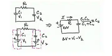
3. Filter Topologies and Component Placement
3.1 Basic EMI Filter Architecture
A practical EMI filter combines multiple filtering elements to address both interference modes. The canonical topology includes:
- Common-mode choke: Coupled inductor providing high impedance to common-mode currents while allowing differential signals
- Differential-mode chokes: Series inductors blocking high-frequency differential noise
- X capacitors: Line-to-line capacitors shunting differential-mode interference
- Y capacitors: Line-to-ground capacitors providing common-mode bypass paths
The effectiveness of each component varies dramatically with frequency and circuit impedance. X capacitors dominate differential-mode attenuation in lower frequency ranges, while Y capacitors become critical for common-mode suppression at higher frequencies.
3.2 Filter Order and Impedance Matching
Filter order, defined by the number of reactive components, directly determines the rejection slope: one reactive element provides 20 dB/decade attenuation, two elements yield 40 dB/decade, and three elements achieve 60 dB/decade. However, component placement relative to source and load impedance proves equally critical.
Starting with a series high-impedance element (inductor) works optimally when the source impedance is low, creating impedance mismatch that reflects noise back toward the source[page:1]. Conversely, starting with a shunt low-impedance element (capacitor) proves effective against high-impedance sources. The attenuation mechanism combines both dissipation in lossy components and reflection from impedance discontinuities.
The general design principle for maximizing filter effectiveness can be expressed mathematically as:
where the reflection component depends on the impedance mismatch ratio:
3.3. Cost Optimization and Component Selection Trade-offs
Filter design inevitably involves balancing performance requirements against cost constraints, particularly in high-volume consumer and industrial applications.
Single-Stage vs. Two-Stage Economics: Single-stage filters typically cost 40–60% less than equivalent two-stage designs while occupying 30–40% less board area. For applications requiring 30–40 dB attenuation, single-stage solutions often suffice. Two-stage filters become cost-effective when alternative approaches (larger single choke, higher capacitance values) exceed space or leakage current budgets.
Integrated Modules vs. Discrete Components: Integrated filter modules command 20–35% price premiums over equivalent discrete implementations but offer significant advantages:
- Pre-certified safety approvals (UL, VDE, CQC) reduce certification time and cost,
- Optimized internal layout minimizes parasitics,
- Reduced assembly labor and simplified BOM management,
- Guaranteed performance matching datasheet specifications.
For production volumes below 10,000 units annually, integrated modules often prove more economical when total cost of ownership (including engineering time, testing, and certification) is considered.
Component Count Reduction Strategies: Careful impedance analysis may reveal opportunities to eliminate redundant components. For example, common-mode chokes with sectional windings provide both common-mode and differential-mode inductance, potentially eliminating separate differential-mode chokes. Similarly, strategic X capacitor placement can reduce total capacitor count by 30–40% while maintaining equivalent attenuation.
Volume Manufacturing Considerations: Custom-designed filters optimized for specific applications can reduce component costs by 15–25% in volumes exceeding 50,000 units annually. However, custom designs sacrifice flexibility and increase inventory risk. Standard catalog modules provide immediate availability, multiple sourcing options, and simplified design reuse across product families.
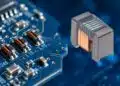
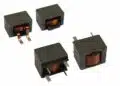
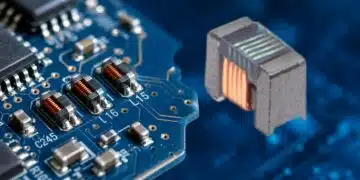
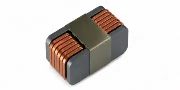
4. Common-Mode Chokes: The Central Filter Component
4.1 Operating Principle and Magnetic Coupling
The common-mode choke represents the most sophisticated component in EMC filter design due to its ability to discriminate between wanted differential signals and unwanted common-mode noise. This selectivity arises from the magnetic coupling between windings on a shared ferromagnetic core.
Perfect symmetry between windings creates complete magnetic flux cancellation for differential-mode currents. When equal currents flow in opposite directions (differential mode), they generate magnetic fluxes of equal magnitude but opposite polarity, resulting in zero net core magnetization. Without core magnetization, no inductance appears, and differential signals pass with minimal impedance.
For common-mode currents flowing in the same direction, magnetic fluxes add constructively, saturating the ferromagnetic core and creating maximum inductance. This inductance generates high impedance that dissipates or reflects common-mode noise while allowing differential signals to pass unimpeded.
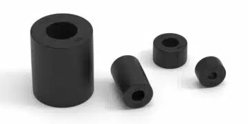
4.2 Core Materials and Frequency Response
Core material selection fundamentally determines the frequency characteristics of common-mode chokes. The complex permeability
describes both flux-conducting ability (real part of μ) and loss characteristics (imaginary part of μ).
Enhanced Core Material Selection Table
This enhanced table provides comprehensive selection criteria for EMC choke core materials:
| Core Material | Effective Frequency Range | Permeability (μᵢ) | Curie Temperature | Temperature Stability | Typical Applications |
|---|---|---|---|---|---|
| Manganese-Zinc Ferrite | 10 kHz – 1 MHz | 2,000–15,000 | 140–180°C | Moderate (±20–30%) | Power supply filters, lower-frequency EMC |
| Nickel-Zinc Ferrite | 1 MHz – 100 MHz | 50–1,500 | 130–200°C | Moderate (±15–25%) | High-frequency EMC, RF suppression |
| Nanocrystalline | 10 kHz – 10 MHz | 50,000–100,000 | >600°C | Excellent (±5%) | Wide-bandwidth filtering, automotive, harsh env. |
| Iron Powder | DC – 1 MHz | 10–100 | N/A (metallic) | Good (±10–15%) | Differential-mode inductors, high current |
Selection Guidelines: Choose manganese-zinc for cost-sensitive power supply applications below 1 MHz. Nickel-zinc provides optimal balance for general EMC filtering in the 1–30 MHz range. Nanocrystalline offers superior performance for automotive and wide-temperature applications despite higher cost, with exceptional bandwidth and thermal stability.
For power inductor applications, engineers typically operate one decade below the resonant frequency to minimize core losses and maintain efficiency. EMC choke design inverts this principle: maximum losses occur precisely where filtering is required, making “poor” power inductor materials ideal for EMC applications.
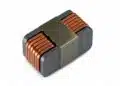
4.3 Winding Styles and Parasitic Effects
Winding configuration significantly impacts both common-mode performance and differential-mode rejection. Two primary styles exist:
Bifilar winding: Both conductors wound together simultaneously, providing maximum symmetry and minimal differential-mode leakage inductance. The tight coupling results in excellent common-mode attenuation with negligible differential-mode impedance.
Sectional winding: Windings placed in separate sections of the bobbin, creating intentional asymmetry. This reduced symmetry generates significant leakage inductance, providing substantial differential-mode attenuation in addition to common-mode suppression.
The leakage inductance Lleak in sectional windings arises from imperfect magnetic coupling and can be estimated as:
where k represents the coupling coefficient (k = 0.999 for bifilar, k ≈ 0.95-0.98 for sectional).
5. Component Selection Methodology
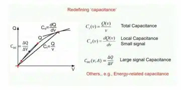
5.1 Beyond Inductance Value: Frequency-Dependent Parameters
Specifying a common-mode choke solely by inductance value (e.g., “1 mH”) provides insufficient information for filter design. The inductance measurement at low frequency (typically 1 kHz or 100 kHz) indicates only the initial slope of the impedance curve, revealing nothing about behavior in the critical EMC frequency range.
Effective component selection requires examining the complete impedance-versus-frequency characteristic, which encompasses:
- Low-frequency inductance region (inductive reactance dominates)
- Mid-frequency loss region (core losses create resistive impedance)
- High-frequency capacitive region (inter-winding capacitance creates resonance)
The impedance magnitude |Z| of a choke can be approximated across frequency as:
where Leff decreases with frequency as the core permeability drops, and Rloss increases due to core losses in lossy ferrite materials.
5.2 Rated Current and Thermal Considerations
The rated current specification for common-mode chokes reflects thermal limits rather than magnetic saturation. Manufacturers typically specify rated current as the DC current (flowing through both windings simultaneously) that produces a defined temperature rise, commonly 40K above ambient.
This measurement methodology ensures the rated value directly corresponds to application conditions. Derating curves extend operation to elevated ambient temperatures; for instance, operation at 90°C ambient might require derating to 80% of the rated current to prevent exceeding the maximum operating temperature of 125-140°C.
Thermal Impedance and Heat Dissipation
Beyond simple rated current specifications, understanding thermal behavior enables accurate worst-case analysis and derating strategies.
Thermal Resistance Path: Heat generated in choke windings follows a thermal path through multiple interfaces:
For typical manganese-zinc ferrite common-mode chokes, the total thermal resistance from winding to ambient air ranges from 25–40°C/W for small surface-mount components to 8–15°C/W for larger through-hole designs with exposed ferrite surfaces.
Power Dissipation Calculation: Winding resistance varies with temperature according to the copper temperature coefficient (0.393%/°C). At elevated temperatures, resistance increases substantially:
A choke with 20 mΩ DCR at 25°C increases to 29 mΩ at 125°C, representing a 45% resistance increase. Power dissipation at rated current becomes:
Derating Methodology: Component datasheets typically provide derating curves showing allowable current versus ambient temperature. Linear derating from rated current at 40°C ambient to 50% rated current at maximum ambient (often 85–100°C) provides conservative operation. For mission-critical applications, limit temperature rise to 30 K rather than the standard 40 K specification to extend component lifetime.
Potted Assembly Considerations: Encapsulation in epoxy or polyurethane potting compounds improves thermal conductivity to enclosure walls but adds thermal mass that slows transient thermal response. Potted assemblies typically exhibit 30–50% lower thermal resistance than air-cooled equivalents, enabling higher current ratings in the same footprint.
5.3 Saturation in Common-Mode Applications
Unlike differential-mode inductors, common-mode chokes exhibit negligible saturation concerns in typical applications. The field cancellation mechanism means differential-mode currents (which may be several amperes) do not magnetize the core significantly.
Common-mode currents remain in the microampere to milliampere range in properly designed systems. A choke might show 20% inductance loss (conventional saturation definition) at only 5 mA common-mode current, yet this poses no practical limitation since normal common-mode currents remain far below this level. Any system with multi-milliampere common-mode currents exhibits serious imbalance problems beyond simple EMC concerns.
6. Capacitor Selection and Safety Considerations
6.1 X Capacitors: Differential-Mode Filtering
X capacitors connect line-to-line (or line-to-neutral) and provide low-impedance shunt paths for differential-mode noise. Their effectiveness increases with frequency as capacitive reactance decreases according to:
X capacitor selection involves balancing several requirements:
- Capacitance value: Larger values provide better high-frequency attenuation but increase standby power consumption and discharge resistor losses
- Voltage rating: Must exceed peak line voltage with adequate safety margin
- Safety class: X1 (≤4 kV impulse) or X2 (≤2.5 kV impulse) classification per IEC 60384-14
- Discharge requirements: Regulations mandate X capacitors discharge to safe voltages (<50V) within specified times after disconnection, necessitating parallel discharge resistors
6.2 Y Capacitors: Common-Mode Filtering and Leakage Current
Y capacitors connect line-to-ground and provide essential common-mode noise bypass paths. However, their usage faces strict limitations due to safety ground leakage current concerns. Even at line frequency (50/60 Hz), Y capacitors conduct leakage current:
where CY represents the total Y capacitance to ground.
Safety standards (IEC 60950, IEC 60065, IEC 60335) limit leakage currents to prevent shock hazards if ground connections fail. Medical equipment faces particularly stringent limits (typically <100 μA). These constraints restrict Y capacitor values, often limiting total Y capacitance to 2-4.7 nF for 230V applications.
Y capacitor safety classification (Y1, Y2, Y3, Y4) depends on insulation requirements and rated impulse voltages per IEC 60384-14, which supersedes the older IEC 60939 reference for safety capacitor specifications.
7. Practical Filter Design Example: RS-485 Interface Protection
7.1 Design Requirements and Constraints
Consider designing an EMC filter for an RS-485 communication interface with the following specifications:
- Line impedance: 60Ω per conductor (120Ω differential)
- Maximum cable length: 1.2 km
- Signal bandwidth: DC to 15 MHz
- Required common-mode attenuation: Sufficient to meet EMC standards starting at 62.5 kHz
- Maximum acceptable differential-mode attenuation: 3 dB at 15 MHz
The 1.2 km cable length creates an efficient antenna at approximately 62.5 kHz (λ/4 ≈ 1200m for 62.5 kHz). Common-mode noise coupling to this cable antenna motivates the filter design.
7.2 Component Calculations
The 3 dB differential-mode attenuation limit at 15 MHz constrains the total differential-mode capacitance. For a π-filter topology with impedance Z0 = 120Ω, the maximum differential-mode capacitance can be calculated from:
Solving for capacitance at f = 15 MHz:
This constraint must account for all differential-mode capacitances:
- X capacitors (intentional)
- TVS diode junction capacitance
- Y capacitor differential-mode component (Y capacitors exhibit differential-mode impedance despite ground connection)
For the example design, selecting X capacitors and considering parasitic contributions yields total differential-mode capacitance of 178 pF, safely below the 181 pF limit.
7.3 Simulation and Validation
LTSpice simulation using manufacturer-provided component models including parasitic elements produces attenuation curves closely matching measured filter performance. The simulation workflow includes:
- Import component models with parasitic inductances, resistances, and capacitances
- Construct filter schematic with appropriate source and load impedances
- Perform AC analysis sweeping from 10 kHz to 100 MHz
- Extract common-mode and differential-mode insertion loss
- Compare simulation to measured performance using network analyzer
The design example achieved excellent agreement between simulation and measurement for differential-mode performance, with some deviation in common-mode response due to component tolerances and layout parasitics.
Advanced Simulation Techniques Beyond LTSpice
While LTSpice provides excellent circuit-level simulation, comprehensive EMC filter validation benefits from additional simulation methodologies.
3D Electromagnetic Field Simulation: Tools such as Ansys HFSS, CST Microwave Studio, or Keysight EMPro solve Maxwell’s equations in three dimensions, capturing effects impossible to represent in lumped-element circuit models:
- Near-field coupling between filter input and output traces,
- Radiated emissions from filter components and PCB traces above 100 MHz,
- Slot antenna effects from ground plane discontinuities,
- Resonant cavity modes in shielded enclosures.
For applications above 30 MHz or in compact enclosures where coupling dominates filter performance, 3D EM simulation identifies layout-dependent degradation mechanisms.
Parasitic Extraction from PCB Layout: Modern PCB design tools (Altium Designer, Cadence Allegro, Mentor Graphics PADS) include parasitic extraction engines that compute trace inductance, inter-trace capacitance, and via impedances from physical geometry. Exporting these extracted networks to SPICE simulators reveals layout-dependent resonances and attenuation nulls not visible in schematic-only simulation.
Monte Carlo Tolerance Analysis: Component tolerances (±10–20% for inductors, ±20% for Y capacitors, ±10% for X capacitors) combine statistically to affect filter performance. Monte Carlo simulation runs thousands of iterations with randomized component values drawn from specified distributions, generating statistical performance bounds. This analysis identifies critical components requiring tighter tolerance specification.
Coupled Thermal-Electrical Simulation: Advanced simulation couples electrical circuit models with finite element thermal analysis. These coupled simulations predict component temperature rise under worst-case electrical stress, enabling accurate derating validation and thermal runaway prediction in high-power filter designs exceeding 1 kW.
7.4. Additional Case Study: Multi-Kilowatt AC-DC Power Supply
To complement the RS-485 communication interface example, consider a more demanding application: a 3 kW industrial AC-DC converter operating from 230 VAC three-phase mains.
Design Requirements:
- Input voltage: 230 VAC three-phase (400 V line-to-line)
- Output: 48 VDC, 62.5 A continuous
- Switching frequency: 65 kHz with spread spectrum modulation
- Target: CISPR 32 Class B compliance with 10 dB margin
- Maximum leakage current: 3.5 mA per IEC 60950
Design Challenges: High power levels generate substantial differential-mode currents at the fundamental switching frequency and harmonics. The filter must handle 4.3 A RMS per phase continuously while providing 40–50 dB attenuation starting at 150 kHz. Y capacitor sizing becomes critical, as the 400 V line-to-line voltage demands Y1-rated components.
Component Selection: The design employs a two-stage filter topology. The first stage uses a common-mode choke with nanocrystalline core rated for 10 A, providing flat impedance from 10 kHz to 10 MHz. X capacitors total 470 nF per stage (940 nF total) for differential-mode suppression, while Y capacitors are limited to 2.2 nF each (4.4 nF total to ground) to maintain leakage current below 3.5 mA:
Thermal Management: At 10 A continuous current, the choke winding resistance (typically 15–25 mΩ) dissipates 1.5–2.5 W per phase. Proper heat sinking and derating to 80% rated current at 70°C ambient ensures reliable operation without exceeding the 140°C maximum winding temperature.
Validation Results: Pre-compliance testing showed the two-stage filter achieved 55–62 dB common-mode attenuation from 150 kHz to 30 MHz and 45–50 dB differential-mode attenuation, providing 12–15 dB margin above CISPR 32 Class B limits.
8. Common Filter Design Failures
8.1 Incorrect Component Placement
The most frequent filter failure mechanism involves improper placement relative to noise sources. Consider a typical power supply input path:
AC Inlet → Mains Switch → EMC Filter → AC-DC Converter
If the switch precedes the filter, the wiring between inlet and switch acts as an unfiltered noise coupling path. Inductive coupling between pre-filter and post-filter wiring creates a parasitic bypass around the filter’s high impedance, dramatically reducing effectiveness.
The coupling impedance Zcoupling between parallel conductors separated by distance d and with length l can be approximated as:
where the mutual inductance M ≈ 0.2 × l × ln(d/r) nH for typical geometries. Even modest coupling creates low-impedance noise paths bypassing the filter.
Best practice: Place filters immediately at the enclosure entry point, keeping input and output wiring physically separated and minimizing parallel runs.
8.2 Filter Input/Output Feedback
Routing filter input and output conductors in parallel or in close proximity creates capacitive and inductive coupling that bypasses the filter’s intended isolation. This feedback mechanism effectively shorts out the filter at high frequencies where coupling impedances become significant.
Measurements show that parallel input/output routing can reduce filter effectiveness by 20-40 dB above 10 MHz. Orthogonal routing or physical shielding between input and output sections prevents this degradation.
8.3 Layout Parasitics
PCB trace inductance significantly impacts capacitor effectiveness. A capacitor intended to provide low-impedance shunt paths to ground becomes ineffective if connected through long traces whose inductive reactance dominates:
At the self-resonant frequency:
, the impedance reaches a minimum. Above f0, inductive reactance increases and capacitor effectiveness degrades. A 1 nF capacitor with just 10 nH of trace inductance resonates at only 50 MHz, providing reduced bypassing at higher frequencies.
Mitigation strategies include:
- Minimizing trace lengths to bypass capacitors
- Using wide traces or planes for ground connections
- Placing capacitors as close as possible to connection points
- Employing multiple capacitors in parallel (different values) to extend frequency coverage
PCB Design Guidelines for Optimal Filter Performance
Printed circuit board layout profoundly impacts filter effectiveness, often determining the difference between marginal compliance and robust EMC margins.
Ground Plane Architecture: Solid, continuous ground planes provide the lowest-impedance return path for high-frequency currents. Split ground planes or poorly connected sections force currents through longer paths, increasing loop areas and radiated emissions. For mixed analog-digital designs, single-point grounding at DC transitions to ground plane architecture above 1 MHz where distributed capacitance dominates.
Layer Stackup Optimization: Four-layer boards should place power and ground as adjacent internal layers, creating a tightly coupled plane capacitor that provides inherent decoupling. The typical stackup (Signal – Ground – Power – Signal) maintains controlled impedance for outer-layer traces while maximizing plane coupling. Six-layer designs add dedicated high-speed signal layers between ground planes.
Trace Impedance Control: High-frequency signal paths require constant impedance to prevent reflections that generate EMI. Calculate trace width and spacing to maintain target impedance (typically 50Ω single-ended, 90–100Ω differential) using the PCB stackup parameters. Impedance discontinuities at vias, connectors, or layer transitions create standing waves that radiate.
Capacitor Ground Connection: Multiple short, wide vias directly beneath bypass capacitor pads minimize ground connection inductance. A single via exhibits 1–2 nH inductance; parallel vias reduce this proportionally. The via-to-pad spacing should be minimized, ideally with via-in-pad construction for critical high-frequency decoupling.
Orthogonal Routing Strategy: Route filter input traces perpendicular to output traces rather than parallel. This technique exploits the cos(θ) coupling reduction, where 90° routing provides 20–30 dB less coupling than parallel routing. Separate input and output on opposite board sides when possible.
Guard Rings and Shielding: Ground trace fencing around sensitive circuits provides electrostatic shielding when properly stitched to the ground plane with frequent vias (every λ/10 at the highest frequency of concern). This technique proves particularly effective for isolating analog measurement circuits from switching noise sources.
8.4 Incorrect Mode Filtering
Attempting to filter differential-mode noise with common-mode chokes, or vice versa, yields poor results. Some designers incorrectly substitute two separate inductors for a common-mode choke, expecting similar performance. However, uncoupled inductors provide only leakage inductance benefit (typically <1% of nominal inductance) for common-mode suppression, reducing effectiveness by 40 dB or more.
Proper filter design requires identifying the dominant interference mode through measurement (using current probes or LISNs) and selecting appropriate components.
9. Advanced Design Considerations
9.1 Complete Filter Solutions: CLFS Product Family
Integrated filter modules combine optimized component selection, controlled layout, and safety certifications in compact packages. These assemblies offer three primary topologies:
Single-stage: One common-mode choke, one X capacitor, two Y capacitors – basic filtering for lower attenuation requirements
Advanced single-stage: Additional X capacitor improves differential-mode performance without increasing volume significantly
Two-stage: Two common-mode chokes with intermediate and output X capacitors – maximum attenuation for demanding applications, 40-80 dB additional suppression versus single-stage
The design tradeoff involves balancing rated current against inductance and capacitance values. Higher rated current requires thicker wire, reducing the number of turns possible in a given core size and consequently reducing inductance. This inductance reduction can be partially compensated by increasing Y capacitance (within leakage current limits) to maintain common-mode attenuation.
9.2 Measurement and Characterization
Historical practice measured filter attenuation at 50Ω source and load impedance due to network analyzer limitations. Modern characterization employs S-parameter measurements with variable impedance transformation, enabling accurate prediction of filter performance under actual application impedances.
Online tools like REDEXPERT allow engineers to enter actual source and load impedances, calculating expected filter attenuation based on measured S-parameters. This approach dramatically improves design accuracy compared to assuming 50Ω impedances that rarely match real applications.
Differential vs. Common-Mode Measurement Techniques
Accurate identification of interference modes requires proper measurement setup and probe placement.
Current Probe Methodology: Clip-on RF current probes measure noise currents without breaking conductor paths. For differential-mode measurement, clamp the probe around both conductors together; the probe responds to the net magnetic field from opposing currents. For common-mode measurement, clamp around individual conductors; the probe responds to fields from parallel currents flowing in the same direction.
Two-Probe Separation Method: Using two identical current probes simultaneously enables real-time mode separation. Position one probe around both conductors (differential response) and another around a single conductor (total current). The common-mode component equals the single-conductor measurement minus half the differential measurement.
Spectrum Analyzer vs. EMI Receiver: Spectrum analyzers provide fast qualitative assessment but lack the standardized detectors (quasi-peak, average) required for compliance testing. EMI receivers implement CISPR-specified detection algorithms with precise resolution bandwidth and sweep time. Pre-compliance testing with spectrum analyzers identifies problem frequencies; final certification requires EMI receivers.
| Measurement Parameter | Spectrum Analyzer | EMI Receiver | Application |
|---|---|---|---|
| Detection modes | Peak, RMS | Quasi-peak, average, peak | Pre-compliance vs. certification |
| Resolution bandwidth | Variable, not standardized | CISPR-specified (200 Hz, 9 kHz, 120 kHz) | Frequency-dependent per standard |
| Sweep time | Fast (milliseconds) | Slow (minutes for full scan) | Quick diagnosis vs. compliance |
| Cost | Lower | Significantly higher | Budget considerations |
| Measurement uncertainty | Higher | Specified and calibrated | Informal vs. formal testing |
9.3 Environmental Effects: Temperature and Potting
Core material temperature coefficients significantly affect filter performance across operating temperature ranges. Manganese-zinc ferrite exhibits moderate temperature sensitivity with Curie temperatures of 140-180°C, showing impedance variations of ±20-30% from -40°C to +125°C.
Nanocrystalline materials demonstrate exceptional temperature stability, maintaining nearly constant impedance from -40°C to +180°C with Curie temperatures exceeding 600°C. This stability proves critical for automotive and industrial applications experiencing wide temperature excursions.
Potting compounds encapsulating filter assemblies can mechanically stress ferrite cores during thermal cycling. Low-quality ferrites may exhibit core fracture or significant permeability changes under mechanical stress, degrading filter performance or causing complete failure. Specifying high-quality core materials with robust mechanical properties prevents these failures.
9.4. Design Margins and Future-Proofing Strategies
Robust filter design incorporates appropriate margins to accommodate manufacturing tolerances, component aging, and potential regulatory changes.
Margin Allocation Philosophy: Target filter performance 6–10 dB below regulatory limits rather than designing for exact compliance. This margin accounts for:
- Component tolerance variations (±10–20% for inductors and capacitors),
- Temperature-dependent parameter shifts (±20–30% across -40°C to +125°C),
- Production variations in PCB layout and assembly,
- Measurement uncertainty in compliance testing (typically ±2–4 dB),
- Aging effects over product lifetime (ferrite permeability typically decreases 5–10%).
Frequency Range Extension: Design filter cutoff frequencies one octave below the lowest problematic emission frequency. EMC standards periodically extend upper frequency limits; EN 55032 now specifies measurements to 6 GHz for specific equipment categories, compared to 1 GHz in older standards. Filters effective to 200–300 MHz provide insurance against future regulatory expansion.
Component Qualification Testing: Specify components meeting appropriate reliability standards beyond minimum electrical parameters. For industrial and automotive applications, AEC-Q200 qualification ensures components withstand thermal cycling, mechanical shock, and humidity exposure without performance degradation.
Tolerance Stack-Up Analysis: Perform worst-case tolerance analysis combining maximum component variations in the direction producing minimum attenuation. Monte Carlo simulation with component tolerance distributions reveals statistical performance margins and identifies critical parameters requiring tighter specification.
10. Conclusion
Effective EMC filter design transcends simple component selection, requiring systematic understanding of noise mechanisms, frequency-dependent component behavior, and practical implementation considerations. Key principles for successful filter implementation include:
- Characterize the interference: Identify whether common-mode or differential-mode noise dominates, and determine the frequency range requiring attenuation
- Select components by frequency response: Inductance values alone provide insufficient information; impedance-versus-frequency curves reveal actual performance
- Consider parasitic effects: Real components exhibit capacitances, resistances, and layout-dependent inductances that fundamentally alter filter behavior above 1 MHz
- Optimize placement: Position filters at enclosure entry points, separate input/output wiring, and minimize trace inductances to bypass capacitors
- Validate through simulation and measurement: Use circuit simulation with parasitic-inclusive models, then verify performance with network analyzer measurements under actual impedance conditions
Modern EMC filter design tools, including S-parameter-based characterization and impedance-variable simulation platforms, enable engineers to achieve first-pass design success. Combined with structured design methodology and awareness of common failure modes, these tools reduce development time while producing optimized, cost-effective filtering solutions.
As switching frequencies continue to increase and EMC regulations become more stringent, disciplined filter design methodology becomes not merely advantageous but essential for product success. The investment in proper component selection, layout optimization, and validation yields substantial returns through reduced certification time, lower production costs, and enhanced product reliability.
Ultimately, EMC filters should be treated as engineered subsystems rather than generic catalog add-ons. By combining the structured design methodology outlined in this article with manufacturer application notes and webinars, engineers can move from trial‑and‑error filter selection to predictable, model‑driven design workflows that consistently achieve compliance and robust field performance.
Design Resources and Tools
Modern EMC filter design benefits from sophisticated software tools and component libraries that accelerate development and improve first-pass success rates.
REDEXPERT Design Tool: Würth Elektronik’s free online platform provides filter selection based on actual application impedances rather than 50Ω assumptions. Engineers enter source and load impedance, required attenuation, and frequency range; the tool recommends filter topologies with predicted performance using measured S-parameter data.
Component S-Parameter Libraries: Major manufacturers provide measured S-parameter files (.s2p format) for EMC components, enabling accurate high-frequency circuit simulation. These files capture parasitic effects including self-resonance, ESR, and frequency-dependent impedance that simple RLC models cannot represent.
LTSpice and SPICE Models: Free circuit simulation software combined with vendor-provided component models allows complete filter performance prediction. Effective simulation workflow includes parasitic extraction from PCB layout and worst-case component tolerance analysis.
EMC Filter Design Kits: Modular prototyping boards accepting various choke and capacitor combinations enable rapid hardware iteration. Würth Elektronik, Schaffner, and other manufacturers offer evaluation kits with multiple topology options and measurement guidance.
3D Electromagnetic Simulation: For critical high-frequency applications above 100 MHz, tools like Ansys HFSS or CST Studio extract parasitic coupling between filter input and output and provide realistic layout performance prediction including radiated emissions.
FAQ: EMC Filters – From Component to Design
EMC filters are needed because switching converters and digital circuits generate conducted and radiated interference that can cause failed compliance tests, malfunction of nearby devices, and poor system reliability.
A typical mains EMI filter contains at least one common-mode choke, differential-mode chokes or inductors, X capacitors between lines, and Y capacitors from line to earth, combined to attenuate both common-mode and differential-mode noise.
Differential-mode noise flows in opposite directions in the two conductors and is mainly suppressed by series inductors and X capacitors, while common-mode noise flows in the same direction in both conductors and is mainly suppressed by common-mode chokes and Y capacitors.
Incorrect placement can create unintended low-impedance coupling paths between input and output wiring, allowing noise to bypass the filter through inductive or capacitive coupling and leading to poor attenuation despite a good schematic.
For the intended differential signal, the magnetic flux of the two windings cancels in an ideal common-mode choke, so the differential-mode inductance is only the small leakage inductance and the useful signal passes with minimal attenuation.
Iron powder, manganese-zinc ferrite, nickel-zinc ferrite, and nanocrystalline cores offer different permeability and loss versus frequency, which determines the useful attenuation band and temperature stability of both common-mode and differential-mode chokes.
Two chokes with the same nominal inductance can have very different impedance curves and attenuation because winding style, parasitic capacitances, core material, and temperature behavior strongly affect the high-frequency performance.
Typical mistakes include using the wrong filter order, placing capacitors behind long inductive traces, routing input and output in parallel, relying on capacitors instead of inductors for low-frequency noise, and ignoring component saturation or parasitics.
This webinar presents a modular EMC filter design kit and simulation models, which allow engineers to assemble different topologies, test them in the real application, and correlate measurements with SPICE-based simulations to converge on a compliant design.
Consumer, industrial, automotive, and military products fall under different EMC frameworks such as CISPR 32, CISPR 25, IEC 61000, and MIL‑STD‑461, each with its own limits, frequency ranges, and measurement setups. Filters must be designed and validated against the specific standard that applies to the target market and installation environment.
GaN and SiC switches have much higher dV/dt and switching frequencies than silicon, shifting interference to higher harmonics and making common‑mode capacitances more critical, so filters must provide effective attenuation well beyond 30 MHz and pay close attention to layout and parasitics.
How-to: Design and Implement an Effective EMC Filter
- Step 1 – Identify EMI sources and limits
Determine the main switching frequencies, harmonics, and relevant EMC standards for your product (for example CISPR 32 for IT/multimedia, CISPR 25 for automotive, or MIL‑STD‑461 for defense), focusing on conducted emissions between 150 kHz and 30 MHz and radiated emissions above 30 MHz.
- Step 2 – Separate common-mode and differential-mode needs
Analyze whether failing frequencies are dominated by common-mode or differential-mode currents so you can size common-mode chokes, differential-mode inductors, and capacitors appropriately.
- Step 3 – Select core materials and choke types
Choose core materials such as manganese‑zinc ferrite or nanocrystalline for common‑mode chokes to obtain high losses in the noise band, and select suitable iron powder or ferrite cores for differential inductors with adequate saturation margin. For GaN or SiC‑based converters with very fast edges, prefer core and winding configurations that maintain effective impedance into the tens or hundreds of megahertz.
- Step 4 – Define X and Y capacitors
Calculate X capacitors for differential-mode attenuation at the lowest problematic frequencies and choose Y capacitors to boost common-mode attenuation while keeping leakage current within the limits of safety standards like IEC 60939.
- Step 5 – Check attenuation versus insertion loss
Evaluate filter transfer functions in SPICE or vendor tools, ensuring that the insertion loss at the wanted signal or mains frequency stays within acceptable limits while providing sufficient attenuation in the rejection band.
- Step 6 – Optimize PCB layout and wiring
Place the filter close to the connector, keep input and output conductors physically separated, minimize loop areas, and avoid routing input and output in parallel to reduce unintended inductive or capacitive coupling paths.
- Step 7 – Prototype with a configurable filter board
Use an EMC filter design kit or modular PCB to combine different chokes and capacitors, then measure conducted emissions to validate whether the chosen topology meets margin goals across the full frequency range.
- Step 8 – Verify thermal behavior and saturation
Confirm that common-mode and differential-mode chokes operate below their rated current and temperature derating curves so that inductance and attenuation do not collapse during worst-case load and ambient conditions.
- Step 9 – Iterate based on EMC test results
If pre-compliance or final lab tests reveal residual peaks, refine the filter order, adjust component values, or change core material and layout until the emissions remain below limits with comfortable design margin.
References
- Würth Elektronik – EMC Filters Explained / Webinar
Original webinar and application material forming the basis for this article.
https://www.we-online.com/ - CISPR 32 / EN 55032 – Electromagnetic compatibility of multimedia equipment
Conducted and radiated emission limits for information technology and multimedia devices.
https://webstore.iec.ch/ - IEC 61000 Series – Electromagnetic Compatibility (EMC)
General EMC framework covering immunity, emissions, and test methods (including IEC 61000‑4‑6 for conducted immunity).
https://webstore.iec.ch/ - CISPR 25 – Radio disturbance characteristics for the protection of receivers in vehicles and boats
Automotive conducted and radiated emission limits and test methods.
https://webstore.iec.ch/ - IEC 60384‑14 – Fixed capacitors for use in electronic equipment – Part 14: Sectional specification – Fixed capacitors for electromagnetic interference suppression and connection to the supply mains
Defines X and Y safety capacitor classes and impulse ratings.
https://webstore.iec.ch/ - MIL‑STD‑461 – Requirements for the Control of Electromagnetic Interference
EMC requirements for defense and aerospace systems, including conducted and radiated emissions and susceptibility.
https://quicksearch.dla.mil/ - AEC‑Q200 – Stress Test Qualification for Passive Components
Automotive qualification requirements for inductors, capacitors, resistors, and other passive components.
https://www.aecouncil.com/ - REDEXPERT – Würth Elektronik Online Design Tool
Web-based platform for selecting EMC chokes and capacitors based on measured S‑parameters and real application impedances.
https://redexpert.we-online.com/ - Coilcraft – A Guide to Understanding Common Mode Chokes
Application note explaining common‑mode choke selection, impedance curves, and frequency behavior.
https://www.coilcraft.com/en-us/edu/series/a-guide-to-understanding-common-mode-chokes/ - PCB Design Guidelines for EMI Reduction
Modern PCB EMI layout guidelines covering stackup, grounding, and filtering practices.
https://resources.pcb.cadence.com/blog/2024-pcb-design-guidelines-for-emi