


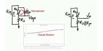
This article provides a step-by-step method to calculate the required capacitance, verify ripple and transient criteria, and choose technology and configuration for robust, manufacturable designs. Robert Feranec in this video discusses with Ali Shirsavar, Biricha how to calculate and choose output capacitor for switching power supplies.
Key Takeaways
- This article outlines a detailed method for Output Capacitor Calculation in switching power supplies, focusing on performance and reliability.
- Key considerations include voltage dip, ripple, equivalent series resistance (ESR), and balancing the capacitor’s type and value.
- Calculate the required capacitance by defining targets, verifying ripple and transient responses, and selecting suitable technology, such as ceramics or electrolytics.
- Follow component placement best practices to minimize impedance and ensure stability, such as placing capacitors near the output inductor.
- Using a hybrid capacitor bank improves performance, balancing bulk energy needs with low ESR for stable operation under varying conditions.
Introduction
Switching power supplies are widely utilized in modern electronic devices due to their efficiency and performance. Among the critical components within these systems is the output capacitor, which plays a pivotal role in maintaining output voltage stability and minimizing ripple.
The output capacitor in a switching power supply (buck, boost, flyback, etc.) shapes load-transient behavior, output ripple, loop stability, and reliability. Selecting its value and type requires balancing voltage deviation limits, transient energy needs, ripple attenuation, equivalent series resistance (ESR), bias effects, and lifetime.
The primary functions of output capacitors in power supplies are:
- Reducing Output Voltage Dip: Mitigates voltage drops when sudden load changes occur before the control loop compensates.
- Minimizing Ripple: Smoothens the ripple current from inductors, crucial in topologies like buck converters.
Calculating Capacitor Values
Define targets and worst-case conditions
Before calculating capacitance, specify the output voltage tolerance (steady-state and transient), maximum load step, allowed settling time, ambient and operating temperatures, targeted ripple (peak-to-peak), and minimum switching frequency. These system limits drive hard requirements on output capacitance and ESR, and ensure the resulting design meets both electrical and reliability goals.
Capacitance Value Based on Voltage Dip Requirement
The allowable voltage dip (undershoot) and the time until the control loop responds are specified in design requirements. The key equation for minimum output capacitance is:
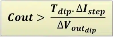
Where:
- Cout = capacitance of the output capacitor
- ΔVout = allowable voltage dip
- ΔIstep = current load step
- Tdip = time period during the Vout will dip
Example calculation:
- A 5V, 2A supply with a 200 kHz switching frequency.
- Allowing 5% dip (250mV) and a 50% load step (1A).
- Time for control loop response = 5 switching cycles (~25 µs).
This results in a minimum required capacitance of 100 µF, adjusted to 150 µF considering a 30-50% safety margin.
Ripple voltage: capacitive reactance and ESR contributions
Output ripple is the sum of the capacitor’s reactive ripple (due to finite capacitance at switching ripple frequency and harmonics) and ESR ripple. Ceramics typically minimize ESR ripple; electrolytics and polymer capacitors have higher ESR but offer bulk energy and improved low-frequency damping. Practical selection targets a combined ripple within the specified peak-to-peak limit.
A simple ESR-dominant estimate for the ripple component is: ΔVESR ≈ Iripple ESR
Where Iripple is the inductor current ripple flowing into the capacitor. In ceramic stacks, the reactive term may dominate, requiring adequate total capacitance and attention to DC bias de-rating.
Technology selection and stacking strategy
- Ceramics (MLCC): Very low ESR/ESL, excellent high-frequency filtering; watch DC-bias de-rating, temperature coefficients, and potential for control-loop peaking without damping.
- Polymer/electrolytic: Provide bulk energy with moderate ESR for damping; suitable for larger step energy and low-frequency ripple control; consider lifetime and temperature grades.
- Hybrid banks: Combine ceramics for HF suppression with polymer/electrolytic for bulk and damping to meet ripple and transient targets with robust stability.
Verification against control loop and inductor slew
Ensure the assumed response time aligns with the regulator bandwidth, modulation type, and inductor current slew rate. If the inductor cannot ramp quickly enough, increase bulk capacitance or relax transient limits. Application notes emphasize cross-checking capacitor impedance across frequency against the regulator’s compensation to avoid instability or excessive peaking.
Detailed insights and calculations
Load-transient energy and capacitance sizing
A refined transient model considers both immediate charge draw and the triangular inductor current ramp during a step. For tight droop limits, include margin for temperature, bias de-rating, and tolerance. Many designs target transient droop at 50–70% of the total voltage budget, leaving headroom for ripple and DC accuracy.
An energy-based perspective: EC = 12 C ( VO2 – VO – ΔV 2 )
This captures the energy the capacitor can deliver for a given allowable droop ΔV. Matching EC to the load step’s energy deficit during control response refines the minimum required C. Application guides recommend validating such calculations against frequency-dependent impedance and loop dynamics.
Ripple components and frequency-domain view
In continuous-conduction buck converters, the fundamental ripple frequency is the switching frequency. The capacitive reactance term scales with 1/(ωC) and higher harmonics; MLCC arrays reduce impedance at HF, while ESR adds a resistive component that may help damping. Practical design balances low ESR for ripple with sufficient damping to avoid control-loop peaking.
DC bias and temperature de-rating in MLCCs
High-permittivity MLCCs exhibit significant capacitance reduction under DC bias and at temperature extremes. Always apply manufacturer de-rating curves at the operating voltage and temperature to ensure the effective capacitance meets transient and ripple requirements. This is a common source of undersized actual capacitance in production unless margining is applied.
ESR, damping, and stability
Non-negligible ESR introduces a real zero that can improve stability in some topologies. Very low ESR banks may require explicit damping (e.g., small series resistance or polymer/electrolytic parallel) to prevent output filter peaking. Check your regulator’s compensation guidance; vendors often specify minimum ESR or recommend hybrid capacitor banks for stable operation over load and temperature.
Lifetime and reliability considerations
Electrolytic and some polymer capacitors have finite lifetime governed by temperature and ripple current. Size for ripple current rating and thermal rise, choose appropriate temperature class, and verify end-of-life capacitance and ESR changes still meet system limits. This ensures long-term compliance with ripple and transient specifications.
Worked example and tabulated checks
Example assumptions
- Topology: Buck converter
- VO: 5.0 V ±3% steady-state; transient ±5%
- ISTEP: 3 A (0 → 3 A)
- tRESP: 50 μs (loop and inductor ramp)
- ΔVallow (transient): 250 mV
- ΔVripple,pp: 20 mV target
- fSW: 500 kHz
Transient capacitance estimate
Using the charge-based approximation: C ≥ 3 50 10-6 0.25 = 0.0006 F
Result: C ≥ 600 μF effective. This is typically achieved with a polymer/electrolytic for bulk plus MLCCs in parallel to control high-frequency ripple, adjusted for de-rating and tolerance.
Ripple check (ESR-dominant)
If Iripple ≈ 0.5 A at 500 kHz and we target ΔVESR ≤ 10 mV, the total ESR should be ≤ 20 mΩ: ESR ≤ ΔVESR Iripple = 0.01 0.5 = 0.02 Ω
Achieve this with multiple low-ESR MLCCs in parallel (for HF ripple) and one or more polymer/electrolytic capacitors for bulk energy and damping. Verify the combined impedance across frequency against the regulator’s guidance.
Summary table: decision criteria
| Criterion | Design target | Primary lever | Verification |
|---|---|---|---|
| Transient droop | ≤ ΔVallow | Increase C (bulk); improve loop bandwidth | Step-load simulation/measurement |
| Ripple (pp) | ≤ ΔVripple | Lower ESR; add MLCCs; adequate C | Ripple measurement at fSW |
| Stability/damping | No peaking/oscillation | Hybrid bank; ESR floor; compensation | Bode plot / time-domain tests |
| De-rating margins | Capacitance effective in situ | Bias/temperature margins | Datasheet curves, worst-case calc |
| Lifetime | Meets mission profile | Ripple current, temperature rating | Reliability models, vendor tools |
Component selection and layout practices
Capacitor mix and placement
- Near the output inductor and load: Place MLCCs close to the inductor-output node and ground to minimize ESL and loop area.
- Bulk capacitor routing: Keep low-impedance paths to ground; thermally relieve high-ripple parts and consider heatsinking if required.
- Paralleling strategy: Use several MLCCs of varied case sizes to spread self-resonances; add polymer/electrolytic slightly downstream for damping.
These practices reduce high-frequency ripple and avoid resonant peaking, complementing the sizing calculations and stability checks outlined in application guidance.
Validation steps
- Analytical sizing: Compute C from transient requirements; set ESR target from ripple limit.
- Impedance sweep: Evaluate Zout across frequency (vendor models) to check damping and loop interaction.
- Prototype tests: Perform load-step, ripple, and Bode measurements across temperature and voltage.
- Margining: Apply de-rating, tolerances, and aging to ensure compliance over lifetime.
Following an application-note-driven workflow ensures the final design meets performance and reliability goals under real operating conditions.
Conclusion
Sizing the output capacitor is primarily a system-limit problem: define droop and ripple targets, compute minimum bulk capacitance and ESR, then choose a hybrid bank that meets impedance and stability needs in the actual environment. Validate with de-rating, prototype measurement, and lifetime checks. This approach aligns with established application guidance and experienced practice across technologies, ensuring robust power delivery with predictable transients and low ripple.
FAQ: Output Capacitor Calculation for Switching Power Supplies
The output capacitor stabilizes voltage, reduces ripple, and provides energy during load transients. It ensures smooth operation and protects sensitive circuits.
Use the formula C ≥ (Istep × tresp) / ΔVallow. This ensures the capacitor can handle load steps without exceeding voltage deviation limits.
Ripple voltage depends on inductor current ripple, capacitor ESR, and capacitive reactance. Low ESR capacitors reduce ripple, while sufficient capacitance ensures stability.
Ceramic MLCCs are used for high-frequency ripple suppression, while polymer or electrolytic capacitors provide bulk energy storage and damping for stability.
MLCCs lose effective capacitance under DC bias and temperature extremes. Electrolytic capacitors may degrade over time, so de-rating and lifetime checks are essential.
How-to: Calculate and Select Output Capacitor for SMPS
- Step 1: Define design targets
Set ripple limits, transient voltage deviation, load step size, and stability margins. Include worst-case temperature and bias conditions.
- Step 2: Estimate transient conditions to set capacitance requirements
Apply the formula C ≥ (Istep × tresp) / ΔVallow to calculate minimum capacitance needed for load transients.
- Step 3: Check ripple voltage
Calculate ripple due to ESR and capacitance. Ensure ΔVripple stays within specification by selecting low ESR capacitors or parallel arrays.
- Step 4: Select capacitor technology
Combine MLCCs for high-frequency suppression with polymer/electrolytic capacitors for bulk energy and damping. Verify de-rating curves.
- Step 5: Validate stability and lifetime
Check impedance across frequency, confirm control-loop stability, and ensure capacitor ratings meet lifetime requirements under operating conditions.
- Step 6: Prototype and measure
Perform load-step and ripple measurements, validate against design targets, and adjust capacitor mix if necessary.
Related topic links
- Buck Converter Design and Calculation
- SEPIC Converter Design and Calculation
- Boost Converter Design and Calculation
- Flyback Converter Design and Calculation
- Fly-Buck Converter Explained and Comparison to Flyback
- LLC Resonant Converter Design and Calculation
- Switching vs Linear Power Converters Compared
- DC-DC Converter Basic Characteristics and Formulas
- Input filters for DC/DC converters
- Selection of Storage Inductors for DC/DC Converters
- Selection of Capacitors for DC/DC Converters