



Passing a conducted emissions test with a line filter starts with separating the measured noise into its common-mode and differential-mode components, because each mode is attenuated by different filter components. This article summarizes the webinar strategy, from the measurement set-up and mode separation to the design of an optimized single-stage line filter, its safety limits and its installation, for design engineers who need to bring a switch-mode power supply below the conducted emission limits.
The webinar by Würth Elektronik, presented by Lorandt Foelkel and Marco from Emzer, explains where to use a power line filter and a common mode choke and how to choose an optimum filter by separating differential-mode (DM) and common-mode (CM) noise [1]. It combines a theoretical introduction with live experiments on a flyback power supply that fails the test without a filter. The article adds the calculation procedure from the related Würth Elektronik application note [2] and the applicable limits. The scope is single-phase AC mains filters for switch-mode power supplies in the 150 kHz to 30 MHz conducted emission range.
Key Takeaways
- A standard conducted emission measurement shows the total noise on each line, not how much of it is common mode or differential mode; separating the modes shows which filter components will be effective.
- Common mode chokes and Y capacitors attenuate common-mode noise; X capacitors, together with the leakage inductance of the common mode choke or separate DM inductors, attenuate differential-mode noise.
- A single-stage LC line filter rolls off at 40 dB per decade; a cut-off frequency of one tenth of the switching frequency gives about 40 dB at the switching frequency, which includes a margin of about 10 dB for typical designs.
- Y capacitance is limited by the permitted protective-earth leakage current, typically 3.5 mA for common equipment with a protective conductor and far less for medical devices; X capacitors need a discharge resistor.
- A filter that passes the test can still be oversized; a filter designed from the measured CM and DM spectra is usually smaller and cheaper than a generic two-stage filter.
- Noise reduction at the source, especially the Y capacitor across the flyback transformer, and correct filter placement at the mains entry are as important as the filter itself.
Webinar Outline
The webinar runs about one hour, including questions and answers. Its agenda is:
- Fundamentals of filter design and the different behavior of ferrite materials, Lorandt Foelkel (about 6 minutes).
- How a common mode choke (CMC) works and how the line filter affects leakage current, Lorandt Foelkel (about 8 minutes).
- Comparison of different line filters, Lorandt Foelkel (about 10 minutes).
- EMI modes, differential mode versus common mode, Marco from Emzer (about 6 minutes).
- Real-world example: a power supply that fails conducted emissions is evaluated, the DM and CM components are identified, and an optimized filter is designed and tested, Marco from Emzer (about 18 minutes).
Conducted Emission Limits and Measurement
Conducted emissions are the interference voltages that a device returns to the mains through its power cord. They are measured in a defined set-up so that results are reproducible between laboratories.
The measurement uses a line impedance stabilization network (LISN), also called an artificial mains network, between the mains and the equipment under test. It provides a defined RF impedance of 50 µH in parallel with 50 Ω, isolates the measurement from noise on the mains and couples the interference voltage of each line to the receiver [3]. The test set-up and the resulting loop impedances determine which noise paths are excited, so understanding them is a prerequisite for targeted suppression [4].
CISPR 32 for multimedia equipment and CISPR 11 for industrial, scientific and medical equipment define limits from 150 kHz to 30 MHz, measured with a 9 kHz bandwidth and with quasi-peak and average detectors [5], [2]. The FCC applies the same values in 47 CFR 15.107 for devices other than Class A digital devices [3]. Table 1 lists the CISPR 32 limits.
| Frequency | Class A, quasi-peak | Class A, average | Class B, quasi-peak | Class B, average |
|---|---|---|---|---|
| 0.15–0.5 MHz | 79 dBµV | 66 dBµV | 66–56 dBµV | 56–46 dBµV |
| 0.5–5 MHz | 73 dBµV | 60 dBµV | 56 dBµV | 46 dBµV |
| 5–30 MHz | 73 dBµV | 60 dBµV | 60 dBµV | 50 dBµV |
Class B applies to residential environments and is 13 dB to 23 dB stricter than Class A, depending on frequency. The quasi-peak value lies between the peak and the average value and rises when the peak events repeat more often [5]. Pre-compliance measurements often use the faster peak detector first: if the peak values are below the average limit, the device passes both detectors.
Above 30 MHz, interference is assessed as radiated emission with an antenna rather than as conducted emission [1]. In the webinar, failures between 150 kHz and 1 MHz were described as typical for flyback power supplies, whose switching frequencies reach up to about 800 kHz; higher switching frequencies shift the problem to higher frequencies.
Differential-Mode and Common-Mode Noise
The two noise modes travel along different paths and need different filter components. Knowing which mode dominates at the failing frequencies is the key step in the webinar strategy.
Noise Paths
Differential-mode noise flows out on one conductor and returns on the other in the opposite direction, in the same loop as the supply current. In a switch-mode power supply it is generated mainly by the pulsed current drawn from the input capacitor. Common-mode noise flows in the same direction on line and neutral and returns through protective earth or stray capacitance, for example through the capacitance between the switching node and the heat sink or between the primary and secondary windings of the transformer [1], [2].
The X capacitors and DM inductors are effective against differential-mode noise, while the common mode choke and the Y capacitors are effective against common-mode noise [6]. A filter optimized for one mode can be almost ineffective for the other.
Separating the Modes
A conventional EMC receiver measures one line at a time, line or neutral, and shows the total of both modes. This makes filter selection difficult, because the result does not reveal how much of the noise is common mode or differential mode [1], [7]. If the LISN outputs for line, VL,RF, and neutral, VN,RF, are measured simultaneously, the two modes follow from Eq. (1) [2], [7]:
The calculation can be made with a two-channel EMI receiver, with an oscilloscope with FFT and math functions, or with an RF power combiner: a 0° combiner gives the sum and a 180° combiner the difference, and 6 dB is subtracted to account for the factor 1/2 [7], [6]. The set-up must be symmetrical, with RF cables of equal length and quality and identical channel settings, and the vertical scale must avoid clipping, which would corrupt the frequency-domain result [6]. A dual-output LISN is preferred to two single LISNs.
The webinar demonstrated a two-channel receiver with peak, quasi-peak and average detectors per channel according to CISPR 16-1-2, which measures line and neutral simultaneously and displays the CM and DM components in real time between 150 kHz and 30 MHz [1]. The presenters pointed out that common-mode results are particularly sensitive to the set-up and the ground connection, and that their demonstration was not made in a screened room.
How Line Filter Components Work
A single-phase line filter combines a common mode choke with X and Y capacitors. Each component acts mainly on one mode, and the choke also contributes to the other through its leakage inductance.
Common Mode Choke
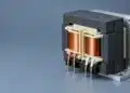
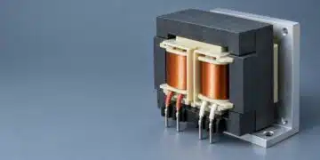
A common mode choke has two identical windings on one core. For a differential current, flowing out through one winding and back through the other, the magnetic fluxes cancel, so the operating current does not saturate the core. For a common-mode current, both windings carry current in the same direction, their fluxes add, and the mutual inductance attenuates the noise [8]. The construction and safe use of chokes in mains filters is described in EMC design fundamentals for varistors and common mode chokes.
Because the coupling of the two windings is not perfect, each winding also has a leakage inductance. This leakage inductance acts on differential-mode current and, together with the X capacitor, forms a DM LC filter [8], [1]. The DM inductance can be read from the differential-mode impedance curve in the datasheet or design tool [2], as shown in the design example below.
Ferrite Core Materials
The core material defines the frequency range in which the choke is effective. Manganese-zinc (MnZn) ferrite has a high permeability and gives high common-mode attenuation in the lower part of the conducted range; chokes such as WE-CMB use it to suppress asymmetrical interference also at low frequencies [9]. Nickel-zinc (NiZn) ferrite has a lower permeability but extends suppression to higher frequencies; WE-CMB NiZn chokes are specified for the middle and high frequency range up to 300 MHz and for burst immunity [10]. A low-capacitance winding technique keeps the choke effective at high frequencies, where interwinding capacitance would otherwise bypass it [9].
X and Y Capacitors
X capacitors are connected between line and neutral and short-circuit differential-mode noise. Y capacitors are connected from line and from neutral to protective earth and return common-mode noise to its source before it reaches the LISN [6]. Both are safety capacitors certified for mains operation, because their failure could cause fire (X) or electric shock (Y); their classes are explained in safety capacitors in power electronics. X capacitors can lose capacitance over their lifetime due to surge pulses and poor mains quality, so a safety margin is needed in the design [2].
Comparing Line Filter Types
Line filters are available as complete modules or can be built from discrete components on the main PCB. The webinar compared both approaches.
Ready-made single-stage filters contain one common mode choke with X and Y capacitors. Two-stage filters add a second choke and further capacitors; they provide higher attenuation but are larger and more expensive [1]. Versions without Y capacitors are available for applications with very low permitted leakage current, such as medical equipment. Catalog insertion loss curves are measured in a 50 Ω system, while the impedances of a real mains network and power supply are different and often asymmetric, so the attenuation in the application can differ from the datasheet [1].
For a discrete design, a filter kit with PCBs, X and Y capacitors and common mode chokes in different core materials allows quick experiments; a varistor and a fuse can be added on the same board [1]. The kit is described in designing EMC line filters with the Würth Elektronik kit. Simulation models of the filter components in LTspice support the pre-selection before the first measurement.
| Filter type | Advantages | Limitations |
|---|---|---|
| Ready-made single-stage module | Tested, certified, quick to integrate; good for moderate excess | Fixed CM and DM ratio; may not match the actual noise spectrum |
| Ready-made two-stage module | High attenuation in both modes; robust margin | Larger, more expensive; often oversized |
| Low-leakage module without Y capacitors | Suitable for medical and other low-leakage equipment | Weaker CM attenuation; CM must be handled by chokes alone |
| Discrete PCB filter | Optimized from the measured CM and DM spectra; smallest and lowest-cost solution | Requires measurement, design effort and own safety qualification |
Designing a Single-Stage Line Filter
The calculation procedure turns the measured excess emission into component values. The example follows the Würth Elektronik application note for an isolated 25 W flyback converter with a switching frequency of 300 kHz, designed for Class B limits.
Required Attenuation
The pre-compliance measurement of the unfiltered converter at maximum load showed CM and DM levels of 84 dBµV at 300 kHz against a 50 dBµV limit, so at least 34 dB of CM insertion loss and 27 dB of DM insertion loss were needed at the switching frequency according to the separate CM and DM measurements [2]. The required attenuation Areq follows from the measured level Vmeas, the limit Vlimit and a safety margin, Eq. (2):
If no measurement is available, the application note recommends designing for at least 40 dB of CM and DM insertion loss at the switching frequency, which includes a margin of about 10 dB. If the switching frequency lies below 150 kHz, the first harmonic inside the measured range is used instead, for example the third harmonic at 210 kHz for a 70 kHz converter [2].
Cut-off Frequency
A single-stage LC filter is a second-order filter with an ideal slope of 40 dB per decade. The attenuation Afsw at the switching frequency fsw and the required cut-off frequency fCO are related by Eq. (3) [2]:
For 40 dB at 300 kHz, Eq. (3) gives fCO = 30 kHz. The same cut-off frequency is used for the CM and the DM filter.
Common Mode Choke Inductance
For common-mode noise, the two Y capacitors CY act in parallel, CYG = 2·CY. With two 4.7 nF Y2 capacitors, CYG = 9.4 nF, and the required CM inductance LCM follows from Eq. (4) [2]:
The result is 3.0 mH. The next standard value, 3.3 mH, is selected, which also covers part of the relatively wide inductance tolerance of common mode chokes; it moves the CM cut-off to 28.6 kHz and gives a calculated CM insertion loss of 41 dB at 300 kHz [2].
Leakage Inductance and X Capacitor
The DM inductance LDM is the leakage inductance of the selected choke. It is obtained from the inductive, linearly rising part of the differential-mode impedance curve: the example choke shows XL = 92 Ω at fDM = 1 MHz, so Eq. (5) gives 14.6 µH [2]:
The X capacitance CX for the same cut-off frequency follows from Eq. (6):
The calculated value is 1.93 µF. A 2.2 µF / 310 V X2 capacitor is selected, which places the DM cut-off at 28.1 kHz and gives a calculated DM insertion loss of 41 dB at 300 kHz [2]. Table 3 summarizes the example; all values were recalculated with the equations above.
| Parameter | Calculated | Selected | Result |
|---|---|---|---|
| Cut-off frequency fCO | 30 kHz | – | 40 dB at 300 kHz |
| Y capacitors CY, CYG | – | 2 × 4.7 nF Y2, 9.4 nF | Limited by leakage current |
| CM inductance LCM | 3.0 mH | 3.3 mH | fCO,CM = 28.6 kHz, 41 dB |
| DM (leakage) inductance LDM | 14.6 µH (92 Ω at 1 MHz) | given by choke | – |
| X capacitor CX | 1.93 µF | 2.2 µF / 310 V X2 | fCO,DM = 28.1 kHz, 41 dB |
The calculated insertion loss assumes ideal components. Self-resonance of the choke and the capacitors and the real source and load impedances reduce the attenuation at higher frequencies, so the filter must be verified by measurement.
Leakage Current and Discharge Resistor
Two safety calculations limit the filter design. The Y capacitors determine the leakage current to protective earth, and the X capacitors must be discharged after the plug is pulled.
Leakage Current
Larger Y capacitors improve common-mode attenuation but increase the leakage current to protective earth. Permitted values range from a few microamperes in medical equipment to many milliamperes in permanently installed industrial systems; 3.5 mA is a common limit for equipment with a protective conductor [2]. In the worst case, with an interrupted neutral or protective earth, the X capacitors appear in series with the neutral-side Y capacitor, which gives Eq. (7) for line voltage VGRID and line frequency fGRID [2]:
For two 1 µF X capacitors and two 5.6 nF Y capacitors at 230 V / 50 Hz, with +10 % line voltage and +20 % capacitance tolerance applied to the X capacitors, the application note calculates 0.89 mA [2]. Applying the +20 % tolerance also to the Y capacitors gives 1.07 mA, still well below 3.5 mA. The applicable product safety standard defines the limit and the measurement method.
Discharge Resistor for X Capacitors
X capacitors stay charged after the plug is disconnected. Safety standards for pluggable equipment, such as IEC 62368-1 and IEC 60335, require the accessible voltage at the plug pins to fall to a safe value within a defined time; the application note uses 60 V within 1 s [2]. The total capacitance Ctot includes the X capacitors, the varistor capacitance and the series connection of the Y capacitors. Because the plug can be pulled at the voltage peak, the initial voltage is the peak line voltage Vpeak, and the discharge resistance Rdis must satisfy Eq. (8):
With Ctot = 2.52 µF (2.1 µF + 20 %), Vpeak = √2 × 253 V = 358 V, Vdis = 60 V and tdis = 1 s, the resistance must be below 222 kΩ. A 200 kΩ resistor discharges the capacitors to 60 V in 0.90 s and dissipates 0.32 W at 253 V. The resistor, or a series chain of resistors, must also meet the required dielectric strength, creepage and clearance distances. Where standby losses matter, X-capacitor discharge ICs disconnect the resistor during operation.
The discharge resistor is part of every filter with X capacitors. The webinar emphasized that its value must be calculated for both the discharge time and the permanent power loss, rather than chosen arbitrarily.
Reducing Noise at the Source in Flyback Converters
The flyback converter is the most common isolated topology below about 100 W, and the webinar used it as the demonstration object. Several design measures reduce its common-mode noise before it reaches the filter.
The parasitic capacitance between the primary and secondary windings couples the switching node voltage across the isolation barrier and drives common-mode current through the secondary ground and protective earth. A Y capacitor of typically up to 4.7 nF from the primary to the secondary ground, placed very close to the transformer pins and rated for the required isolation voltage, returns this current locally [1]. In the demonstration, the common mode choke alone reduced the noise but was not enough to pass; adding and adjusting the Y capacitor across the transformer brought the supply below the limit [1].
Transformer construction influences both the interwinding capacitance and the leakage inductance. Separating the windings reduces the capacitance but increases the leakage inductance, which requires a stronger snubber and reduces efficiency. An interleaved, or sandwich, winding of primary, secondary and primary gives a balance of both [1]. The trade-off is analyzed in transformer interwinding capacitance versus leakage inductance.
The webinar also showed that the winding start, or dot, connected to the switching node reduced EMI in the tested design, and that fully potting the transformer increased emissions compared with an unpotted version in the same converter [1]. Transformer leakage inductance, PCB parasitics and the MOSFET capacitance cause overshoot and ringing at turn-off; an RC snubber and, where needed, a TVS or Zener clamp limit the peak voltage, as described in RC snubber design for SMPS protection.
Filter Installation and Layout
Even an optimally designed filter fails if noise can bypass it. The webinar stressed several installation rules.
- Place the line filter as close as possible to the mains entry or connector [1].
- Keep filtered and unfiltered wiring apart. Crossing them or routing them in parallel couples noise around the filter and cancels its effect.
- Provide a low-impedance, short connection between the filter ground and the chassis or protective earth; a long ground wire adds inductance in series with the Y capacitors.
- Use pulse-rated power ferrite beads on the primary side if beads are added; standard signal beads are not designed for mains surges.
- Twisting the mains wires is not a substitute for a filter.
- If an integrated power supply cannot be modified, place a filter in front of it or select a supply with better EMC performance.
Real-World Example from the Webinar
The live demonstration compared ready-made filters with a filter designed from the separated CM and DM spectra. It illustrates why the mode separation pays off.
Without a filter, the power supply exceeded the limit. A large ready-made filter brought the total emission below the limit, but the presenters noted that it was probably too large and expensive for the product. A smaller filter module improved common-mode attenuation over parts of the spectrum but performed worse in differential mode, which a single total-emission measurement would not have revealed [1].
A discrete PCB filter designed from the separated spectra reduced the common-mode emission by about 60 dB at the lower frequencies and also reduced the differential-mode emission substantially, leaving a margin of about 40 dB in the overall measurement with a smaller filter than the ready-made module [1]. The general rule from the questions and answers was to identify the mode and the frequencies first and then choose components that are effective at those frequencies; an unsuitable capacitor can waste money and even increase emissions.
Line Filter Design Checklist
The checklist summarizes the steps and datasheet parameters to compare when a power supply must be brought below the conducted emission limits.
- Standard and class: CISPR 32, CISPR 11 or the applicable product standard, Class A or Class B, quasi-peak and average limits.
- Measurement: unfiltered reference at maximum load, simultaneous line and neutral measurement, CM and DM spectra separated with Eq. (1).
- Target: required CM and DM attenuation at the switching frequency or its first harmonic above 150 kHz, plus about 10 dB margin.
- Common mode choke: CM inductance and tolerance, leakage inductance from the DM impedance curve, rated current, DC resistance, core material, winding capacitance and safety approvals.
- X capacitor: X1 or X2 class, rated voltage, capacitance stability over lifetime, discharge resistor value and power.
- Y capacitor: Y1 or Y2 class, leakage current against the applicable limit, including the transformer Y capacitor.
- Catalog versus custom: ready-made modules for speed and certification; discrete PCB filters for size and cost once the spectra are known.
- Installation: filter at the mains entry, separated input and output wiring, short ground connection.
- Verification: final compliance test in an accredited laboratory, as pre-compliance set-ups can differ by several decibels.
Conclusion
Passing conducted emissions efficiently means measuring before filtering. A simultaneous measurement of line and neutral, separated into common-mode and differential-mode spectra, shows whether the common mode choke and Y capacitors or the X capacitors and leakage inductance must do the work, and at which frequencies.
With the required attenuation known, a single-stage filter is dimensioned from the cut-off frequency at about one tenth of the switching frequency, within the leakage-current limit for the Y capacitors and with a correctly calculated discharge resistor for the X capacitors. Combined with source measures in the flyback transformer and a clean installation at the mains entry, this approach typically gives a smaller and less expensive filter than a generic two-stage module.
FAQ
A standard conducted emission measurement shows the total noise on line or neutral but not which mode causes it. Common-mode noise is attenuated mainly by the common mode choke and Y capacitors, while differential-mode noise is attenuated by X capacitors and the leakage inductance of the choke. Separating the modes shows which components are needed and avoids oversized or ineffective filters.
The line and neutral outputs of a dual LISN are measured at the same time. The differential-mode voltage is half the difference of the two voltages and the common-mode voltage is half their sum. The calculation can be made with a two-channel EMI receiver, an oscilloscope with FFT and math functions, or with 0 and 180 degree power combiners.
A common mode choke has two windings on one core. The operating current flows in opposite directions, so its flux cancels and the core does not saturate. Common-mode noise flows in the same direction in both windings and sees the full inductance. The imperfect coupling also creates a leakage inductance that acts with the X capacitor as a differential-mode filter.
CISPR 32 limits conducted emissions on the AC mains port from 150 kHz to 30 MHz. For Class B, the quasi-peak limit falls from 66 to 56 dBµV between 0.15 and 0.5 MHz, is 56 dBµV up to 5 MHz and 60 dBµV up to 30 MHz. The average limits are 10 dB lower, and the Class A limits are 13 to 23 dB higher.
A single-stage LC line filter attenuates by 40 dB per decade above its cut-off frequency. Setting the cut-off at one tenth of the switching frequency gives about 40 dB at the switching frequency, which covers typical excess emissions plus about 10 dB margin. For a 300 kHz flyback converter, this means a cut-off frequency of 30 kHz for both the common-mode and differential-mode filter.
Y capacitors connect line and neutral to protective earth, so they cause a leakage current at mains frequency. Safety standards limit this current, commonly to 3.5 mA for equipment with a protective conductor and to much lower values for medical equipment. The Y capacitance therefore cannot be increased freely, and common-mode attenuation must come largely from the choke inductance.
X capacitors remain charged after the mains plug is pulled, and the plug pins could then present a dangerous voltage. Safety standards require the voltage to fall to a safe value within a short time, typically below 60 V within about one second. A resistor across the X capacitors provides this discharge, and its value must balance discharge time against continuous power loss.
Yes. A large two-stage filter often passes the test easily but adds size and cost. If the measured spectrum shows that one mode dominates, a single-stage or discrete PCB filter tailored to that mode can achieve the same compliance with fewer and smaller components. The webinar demonstration showed a custom filter outperforming a larger ready-made module.
How to Design a Line Filter to Pass Conducted Emissions
Step-by-step procedure for designing a single-stage line filter that brings a switch-mode power supply below the conducted emission limits.
- Measure the unfiltered reference
Connect the power supply at maximum load to a dual-output LISN and record line and neutral emissions between 150 kHz and 30 MHz without a filter.
- Separate the noise modes
Calculate the common-mode spectrum as half the sum and the differential-mode spectrum as half the difference of the line and neutral voltages.
- Determine the required attenuation
Subtract the applicable limit from the measured CM and DM levels at the switching frequency or its first harmonic above 150 kHz and add about 10 dB margin.
- Calculate the cut-off frequency
Divide the switching frequency by ten to the power of the required attenuation divided by 40 dB, which gives the cut-off frequency of the single-stage filter.
- Select the Y capacitors and common mode choke
Choose Y capacitors within the leakage-current limit and calculate the CM inductance from the cut-off frequency and the parallel Y capacitance, then select the next standard choke.
- Select the X capacitor and discharge resistor
Read the leakage inductance from the DM impedance curve of the choke, calculate the X capacitance for the same cut-off frequency and size the discharge resistor for the required discharge time.
- Install and verify the filter
Mount the filter at the mains entry with separated input and output wiring and a short ground connection, then repeat the CM, DM and total emission measurements.
Further Reading
- AC Line Filter Calculation, Design and LT Spice Simulation: the same design steps verified by circuit simulation.
- AC Line Filters and Insertion Loss Explained: how line filter insertion loss is specified and measured.
- Modular AC Line EMI Filters Explained: construction and selection of ready-made filter modules.
- 3-Phase EMI Filter Design, Simulation, Calculation and Test: extending the method to three-phase systems.
- Flyback Transformer Explained: transformer design of the converter used in the demonstration.
- EMI Filter Online Calculation and Selection with REDEXPERT: tool-based filter dimensioning.
- Introduction to EMI Filtering: insertion loss, filter configurations and the 50 Ω reference.
- RF Inductors and Filters: fundamentals of inductors and LC filters.
References
- How to Pass Conducted Emissions Using Line Filters – webinar recording, Würth Elektronik and Emzer, 2022.
- A. Nadler, S. Klein, ANP015 1-Phase Line Filter Design, Würth Elektronik eiSos, application note, 2024.
- 47 CFR 15.107, Conducted limits, U.S. Federal Communications Commission, Electronic Code of Federal Regulations.
- A. Stirn, SN023 Conducted Emissions Test, Würth Elektronik eiSos, support note, 2024.
- R. Martinez, Z. Zhang, Fundamentals of EMI Requirements for an Isolated DC/DC Converter, Texas Instruments, white paper, 2021.
- Optimizing EMI Input Filters for Switched Mode Power Supplies, GFM353, Rohde & Schwarz, application note, 2021.
- L. Jiang, F. Wang, K. Szolusha, K. Mathews, A Practical Method for Separating Common-Mode and Differential-Mode Emissions in Conducted Emissions Testing, Analog Dialogue, Analog Devices, 2021.
- Common Mode Filter Design Guide, Coilcraft, application note.
- WE-CMB Common Mode Power Line Choke – product page, Würth Elektronik eiSos.
- WE-CMB NiZn Common Mode Power Line Choke – product page, Würth Elektronik eiSos.
- Würth Elektronik – EPCI premium supplier page, Passive Components Blog.
Article revised and technically reviewed in November 2026: expanded the webinar announcement into a technical summary with conducted emission limits, CM and DM separation, line filter components and types, a recalculated single-stage line filter design example, leakage-current and discharge-resistor calculations, flyback source measures, installation rules, checklist, FAQ and How-to, corrected a misdirected link and added referenced sources.