Passive Components Blog
No Result
View All Result
  • Home
  • NewsFilter
    • All
    • Aerospace & Defence
    • Antenna
    • Applications
    • Automotive
    • Capacitors
    • Circuit Protection Devices
    • electro-mechanical news
    • Filters
    • Fuses
    • Inductors
    • Industrial
    • Integrated Passives
    • inter-connect news
    • Market & Supply Chain
    • Market Insights
    • Medical
    • Modelling and Simulation
    • New Materials & Supply
    • New Technologies
    • Non-linear Passives
    • Oscillators
    • Passive Sensors News
    • Resistors
    • RF & Microwave
    • Telecommunication
    • Weekly Digest

    Littelfuse Presents Ultra-Miniature Half-Pitch SMT DIP Switches

    SCHURTER Releases Compact SMT DIP Switches

    TDK and Nippon Chemical Launch Joint Venture for MLCC Materials

    Wk 14 Electronics Supply Chain Digest

    Bourns Releases Compact High Current Shielded Power Inductors

    March 2026 Interconnect, Passives and Electromechanical Components Market Insights

    Molex Completes Acquisition of Smiths Interconnect, Expanding Portfolio of High-Reliability Connectivity Solutions

    APEC 2026 Power Electronics Trends and Implications for Passive Components

    Hydra Enhances Film Capacitor Robustness by Novel Gel Filler

    Trending Tags

    • Ripple Current
    • RF
    • Leakage Current
    • Tantalum vs Ceramic
    • Snubber
    • Low ESR
    • Feedthrough
    • Derating
    • Dielectric Constant
    • New Products
    • Market Reports
  • VideoFilter
    • All
    • Antenna videos
    • Capacitor videos
    • Circuit Protection Video
    • Filter videos
    • Fuse videos
    • Inductor videos
    • Inter-Connect Video
    • Non-linear passives videos
    • Oscillator videos
    • Passive sensors videos
    • Resistor videos

    Transformer-Based Power-Line Harvester Magnetic Design

    Thermal Modeling of Magnetics

    Standard vs Planar LLC transformers Comparison for Battery Chargers

    How Modern Tools Model Magnetic Components for Power Electronics

    Advanced Loss Modeling for Planar Magnetics in the Frenetic Planar Tool

    2026 Power Magnetics Design Trends: Flyback, DAB and Planar

    Enabling Software‑Defined Vehicle Architectures: Automotive Ethernet and Zonal Smart Power

    Calculating Resistance Value of a Flyback RC Snubber 

    One‑Pulse Characterization of Nonlinear Power Inductors

    Trending Tags

    • Capacitors explained
    • Inductors explained
    • Resistors explained
    • Filters explained
    • Application Video Guidelines
    • EMC
    • New Products
    • Ripple Current
    • Simulation
    • Tantalum vs Ceramic
  • Knowledge Blog
  • DossiersNew
  • Suppliers
    • Who is Who
  • PCNS
    • PCNS 2025
    • PCNS 2023
    • PCNS 2021
    • PCNS 2019
    • PCNS 2017
  • Events
No Result
View All Result
Passive Components Blog
No Result
View All Result

Impact of a Decoupling Capacitor in a CMOS Inverter Circuit

30.8.2019
Reading Time: 9 mins read
A A

Source: InCompliance article

by Bogdan Adamczyk. This article discusses CMOS inverter switching and shows the impact of a decoupling capacitor on the power rail signal integrity and radiated emissions.

RelatedPosts

Littelfuse Presents Ultra-Miniature Half-Pitch SMT DIP Switches

SCHURTER Releases Compact SMT DIP Switches

TDK and Nippon Chemical Launch Joint Venture for MLCC Materials

CMOS Inverter Switching

Let’s start our discussion with a CMOS inverter logic gate in a totem-pole configuration, shown in Figure 1 [1].

Figure 1: CMOS Inverter Logic Gate


In high-speed digital circuits, one often encounters the cascaded CMOS configuration shown in Figure 2a. A simplified model of this configuration is shown in Figure 2b.

Figure 2: a) Cascaded CMOS configuration, b) simplified model


Let’s investigate the operation of this configuration on the low-to-high and high-to-low transition of the input to the first inverter.

First, assume that the load capacitors CGP and CGN are initially uncharged. When the input signal IN = Low, the upper transistor is ON and the lower is OFF. The current flows through the upper transistor, signal trace, and the capacitor CGN to ground. This is shown in Figure 3a.

Eventually, the capacitor CGN is charged to (approximately) VCC and the current flow stops, as shown in Figure 3b.

Figure 3: a) Input Signal is Low, b) Current flow stops when CGN is charged to VCC


Now, the driver inverter transitions from low-to-high. Subsequently, the upper transistor turns OFF and the lower transistor turns ON, as shown in Figure 4a.

At this point we have two sources of current:

  1. Current supplied by CGN as it discharges (dashed arrow).
  2. Current supplied by VCC as it charges the upper load capacitor.

The current then flows along the trace towards the driver and through the lower transistor to ground. Eventually, the current flow stops and the voltage across capacitor CGP is VCC. This is shown in Figure 4b.

Figure 4: a) Transition from low-to-high, b) Current flow stops when CGP is charged to VCC


Now, the driver inverter transitions from high-to-low. Subsequently, the upper transistor turns ON and the lower transistor turns OFF, as shown in Figure 5.

Figure 5: Transition from high-to-low


At this point we have two sources of current:

  1. Current supplied by CGP as it discharges (dashed arrow).
  2. Current supplied by VCC flowing through the upper transistor, along the trace, and through the lower load capacitor, eventually charging it to VCC.

Decoupling Capacitor

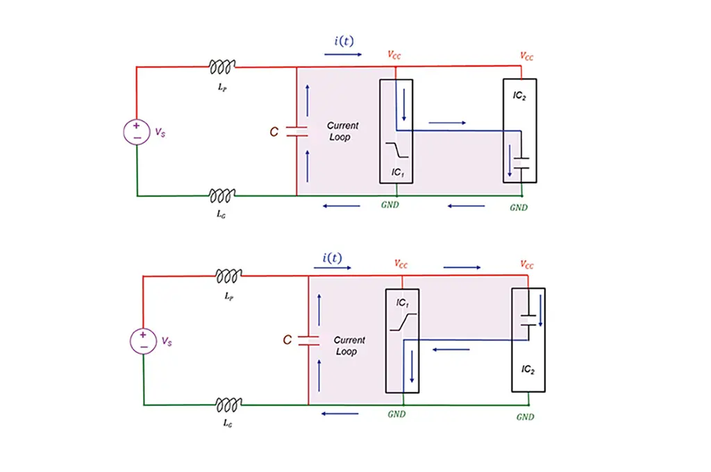
Now let’s turn our attention to a typical scenario in digital logic circuits with a dc voltage source CMOS driver and a load IC, as shown in Figure 6.

Figure 6: CMOS transistors in a high-speed logic circuit


When a CMOS gate switches a current transient is drawn from the power distribution system (PDN). This current flows from the source to the load along the forward path i.e., the power traces and back to the source through the return path i.e., the ground traces.

This time-varying current creates a time-varying magnetic flux that crosses the loop area of the circuit inducing a voltage drop along the traces. We can model this phenomenon by inserting either a voltage source somewhere in the loop, or by inserting an inductance somewhere in the loop. Both the induced voltage and the inductance are distributed along the loop. When the loop is electrically small at the frequencies considered we can model these distributed effects as lumped sources or inductances.

In any practical circuit the forward and return paths (horizontal lines in Figure 9, are orders of magnitude longer than the length of a path between the power and ground pins (vertical lines in Figure 9. It is, therefore, reasonable to insert the lumped parameters only into the forward and return paths. To model the flux-induced effect we will insert inductances along the power and ground traces. This is shown in Figure 7.

Figure 7: Current loop area and partial inductances


This model applies at lower frequencies where the partial inductances of the power and ground traces connecting the ICs themselves can be neglected. At higher frequencies we would augment the model with additional partial and parasitic inductances between the ICs and within the ICs themselves (see [2] for more details).

When the driver IC switches, the current is drawn from the source resulting in the voltages VP and VG across the power and ground inductances. We often refer to these voltages as a power rail collapse and a ground bounce, respectively.

During the off-switching time (dc condition) inductances act as short circuits and the voltage VIC between the driver-IC power and ground pins equals the source voltage VS. During the switching time the voltage VIC no longer equals the source voltage VS potentially causing signal integrity issues. This voltage now equals

  (1)

Additionally, the transient current flows in a large loop creating an efficient loop antenna.

Now, let’s place a capacitor between the power and ground pins near the switching IC, as shown in Figure 8.

Figure 8: Decoupling capacitor placed near the switching IC


During the off-switching time this capacitor charges to the source voltage VS. During the switching time this capacitor ideally supplies the total required current to the load, as shown in Figure 8.

In reality, it supplies most of the current to the load, thus reducing the current draw from the source and consequently reducing the voltage drops across the inductances. Assuming the ideal scenario, the transient current flows now in a smaller loop, as shown in Figure 9. This, in turn, reduces radiated emissions.

Figure 9: Current loop area with a decoupling capacitor


Decoupling Capacitor Impact – Measurements

The measurement setup is shown in Figure 10.

Figure 10: Measurement set-up


The circuit schematic is shown in Figure 11, while the board details are shown in Figure 12.

Figure 11: Circuit schematic
Figure 12: CMOS Inverter board


The board was purposely designed with the very long traces to show the negative impact of the associated inductance, while at the same time increasing the impact of a decoupling capacitor. Figure 13 shows the voltage measurement at the VCC pin of the inverter with no decoupling capacitors.

Figure 13: Voltage at the VCC pin at the inverter – no decoupling caps


Notice the peak-to-peak voltage fluctuations of 1.58 V. Figure 14 shows the voltage measurement at the VCC pin of the inverter with the decoupling capacitors.

Figure 14: Voltage at the VCC pin at the inverter with decoupling caps


Note the dramatic decrease in the voltage fluctuations from 1.52 V to 232 mV. Finally, Figure 15 shows the radiation measurements with and without the decoupling capacitors.

Figure 15: Radiated emissions measurements


References

  1. Bogdan Adamczyk, Foundations of Electromagnetic Compatibility with Practical Applications, Wiley, 2017.
  2. Hubing, Drewniak, Van Doren & Hockanson – Power Bus Decoupling on Multilayer Printed Circuit Boards, IEEE Trans. on EMC, vol. 37, No. 2,
    May 1995

Dr. Bogdan Adamczyk is professor and director of the EMC Center at Grand Valley State University (http://www.gvsu.edu/emccenter) where he develops EMC educational material and teaches EMC certificate courses for industry. He is an iNARTE certified EMC Master Design Engineer. Prof. Adamczyk is the author of the textbook “Foundations of Electromagnetic Compatibility with Practical Applications” (Wiley, 2017). He can be reached at [email protected].

Related

Recent Posts

TDK and Nippon Chemical Launch Joint Venture for MLCC Materials

7.4.2026
7

March 2026 Interconnect, Passives and Electromechanical Components Market Insights

2.4.2026
55

APEC 2026 Power Electronics Trends and Implications for Passive Components

1.4.2026
77

Hydra Enhances Film Capacitor Robustness by Novel Gel Filler

1.4.2026
26

Indias ECMS Wave Brings New Capacity For Passive Components Manufacturing in India

31.3.2026
41

Samsung Introduces 35V MLCCs Flying Capacitors for USB PD Fast Charging

27.3.2026
35

New J‑STD‑075B Standard Elevates Process Sensitivity Classification for Passive and Solid-State Components

27.3.2026
54

Modelithics Expands COMPLETE+3D Library for Ansys HFSS

27.3.2026
9

Equivalent Circuit Constants of Crystal Units Explained

26.3.2026
40

Upcoming Events

Apr 8
17:00 - 18:00 CEST

Trade Secrets of the Flyback Converter

Apr 21
16:00 - 17:00 CEST

Heatsink Solutions: Thermal Management in electronic devices

May 5
16:00 - 17:00 CEST

Understanding and Selecting Capacitors – Fundamentals, Technologies and Latest Trends

View Calendar

Popular Posts

  • Buck Converter Design and Calculation

    0 shares
    Share 0 Tweet 0
  • Boost Converter Design and Calculation

    0 shares
    Share 0 Tweet 0
  • Flyback Converter Design and Calculation

    0 shares
    Share 0 Tweet 0
  • LLC Resonant Converter Design and Calculation

    0 shares
    Share 0 Tweet 0
  • Dual Active Bridge (DAB) Topology

    0 shares
    Share 0 Tweet 0
  • MLCC and Ceramic Capacitors

    0 shares
    Share 0 Tweet 0
  • Capacitor Charging and Discharging

    0 shares
    Share 0 Tweet 0
  • Ripple Current and its Effects on the Performance of Capacitors

    3 shares
    Share 3 Tweet 0
  • Plastic Materials Dielectric Constant and DF

    4 shares
    Share 4 Tweet 0
  • MLCC Case Sizes Standards Explained

    0 shares
    Share 0 Tweet 0

Newsletter Subscription


Passive Components Blog

© EPCI - Leading Passive Components Educational and Information Site

  • Home
  • Privacy Policy
  • EPCI Membership & Advertisement
  • About

No Result
View All Result
  • Home
  • Knowledge Blog
  • PCNS

© EPCI - Leading Passive Components Educational and Information Site

This website uses cookies. By continuing to use this website you are giving consent to cookies being used. Visit our Privacy and Cookie Policy.
Go to mobile version