Passive Components Blog
No Result
View All Result
  • Home
  • NewsFilter
    • All
    • Aerospace & Defence
    • Antenna
    • Applications
    • Automotive
    • Capacitors
    • Circuit Protection Devices
    • electro-mechanical news
    • Filters
    • Fuses
    • Inductors
    • Industrial
    • Integrated Passives
    • inter-connect news
    • Market & Supply Chain
    • Market Insights
    • Medical
    • Modelling and Simulation
    • New Materials & Supply
    • New Technologies
    • Non-linear Passives
    • Oscillators
    • Passive Sensors News
    • Resistors
    • RF & Microwave
    • Telecommunication
    • Weekly Digest

    PCNS 2025 Final Program Announced!

    DigiKey Expands Inventory with Over 32,000 Stocking NPIs in Q2 2025

    YAGEO Offers High-Performance Diplexers for Dual-Band Wi-Fi 6E/7Integration

    European Components Distribution (DMASS) Faces Continued Decline in Q2 2025

    TDK Announced Wide Frequency Automotive Wirewound POC Inductors

    Bourns Released Rugged, High-Power TO-247 Thick Film Resistor

    Bourns Announced Shielded Power Inductor with High Saturation and Low Radiation

    Würth Elektronik Expands MagI³C with Variable Step-Down Modules

    KYOCERA AVX Releases 600MHz Band71 Compact SAW Duplexer

    Trending Tags

    • Ripple Current
    • RF
    • Leakage Current
    • Tantalum vs Ceramic
    • Snubber
    • Low ESR
    • Feedthrough
    • Derating
    • Dielectric Constant
    • New Products
    • Market Reports
  • VideoFilter
    • All
    • Antenna videos
    • Capacitor videos
    • Circuit Protection Video
    • Filter videos
    • Fuse videos
    • Inductor videos
    • Inter-Connect Video
    • Non-linear passives videos
    • Oscillator videos
    • Passive sensors videos
    • Resistor videos

    Switched Capacitor Converter Explained

    Understanding Inductor Dot Markings and Their Application in LTspice

    Accelerating Full Bridge LLC Resonant Converter Design with Frenetic AI

    Understanding Switched Capacitor Converters

    Coupled Inductors Circuit Model and Examples of its Applications

    Inductor Resonances and its Impact to EMI

    Highly Reliable Flex Rigid PCBs, Würth Elektronik Webinar

    Causes of Oscillations in Flyback Converters

    How to design a 60W Flyback Transformer

    Trending Tags

    • Capacitors explained
    • Inductors explained
    • Resistors explained
    • Filters explained
    • Application Video Guidelines
    • EMC
    • New Products
    • Ripple Current
    • Simulation
    • Tantalum vs Ceramic
  • Knowledge Blog
  • Suppliers
    • Who is Who
  • Events
No Result
View All Result
Passive Components Blog
No Result
View All Result

Miniaturization of High Voltage MLCC for Space Applications

5.2.2025
Reading Time: 8 mins read
A A

This article is an excerpt from ESA SPCD 2022 paper entitled “Miniaturization of high voltage MLCC for space applications” written by Pascale ESCURE, Nicolas RUSCASSIER, Tchavdar DOYTCHINOV, EXXELIA SAS, France ( that was presented during the 4th ESA SPCD conference at ESA ESTEC, The Netherlands 11-14th October 2022. Published under ESA SPCD organisation committee permission.

INTRODUCTION

Miniaturization of equipment is a permanent challenge in the space field, for space and weight reduction.

RelatedPosts

Exxelia Offers High-Q RF Microwave Capacitors for High Reliability Applications

Exxelia to Present Smart Integrated Magnetics and MML Film Capacitors at SIAE25 

Exxelia Power Film Capacitors Support Critical Systems Across Various Industries

The challenge with high voltage components used in space application is a breakdown (surface arcing) that can appear at voltage below 350 V.

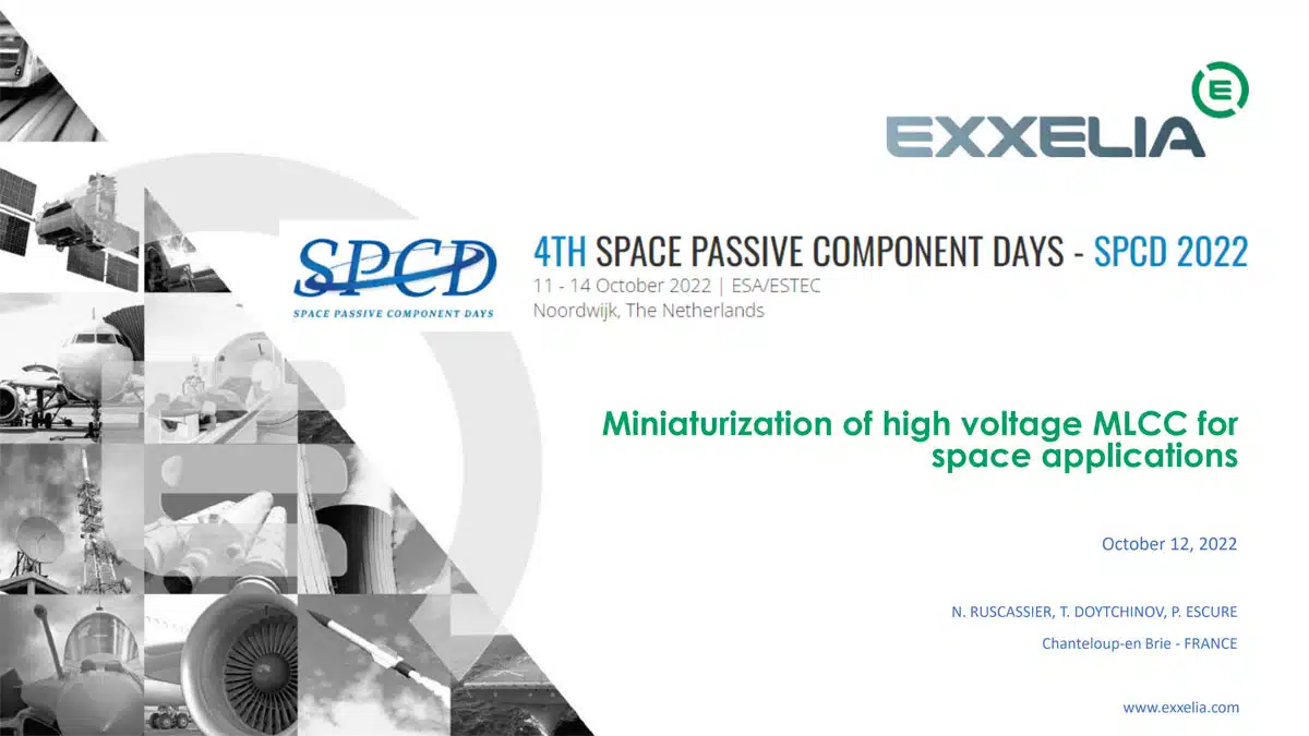
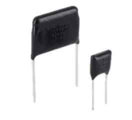
To allow parts size reduction while maintaining optimal reliability and avoid surface arcing, varnishing or molding solutions exist for single leaded ceramic capacitor chips (Figure 1.). For stacked MLCC ceramic capacitors (Figure 2.) however, the arcing risk remains in the areas between the chips elements, because of presence of gas.

Fig.1: Single chip leaded ceramic capacitor
Fig. 2: Stack leaded MLCC ceramic capacitor

BREAKDOWN VOLTAGE IN LOW-PRESSURE GASEOUS ENVIRONMENT

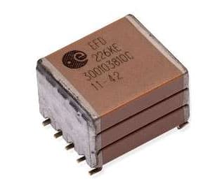
According to the High voltage engineering and design handbook, the basic breakdown mechanism is caused by collision of charge carriers in the gas volume and interactions with the electrode surfaces (Townsend mechanism).

Fig.3.: Breakdown voltage in low-pressure gaseous environment – Paschen curve

In principle, the electrical field accelerates free electrons inside gas-filled gap. These accelerated electrons are colliding with gas atoms.

If the kinetic energy of the electrons is high enough, they ionize gas atoms, releasing further electrons. An avalanche of electrons can grow towards the anode, while the ions moving in opposite direction collide with the cathode releasing new electrons. A well ionized, high conductive breakdown channel can develop in a time frame of a few microseconds. As a consequence of the avalanche breakdown, there is always an optimum, where molecule distance (given by gas pressure) and electrical field strength (given by total gap distance) are providing optimum conditions for ionisation.

For these “optimum” conditions, the result is a very low breakdown voltage (Fig.3.). This physical relation is expressed by the “Paschen Law” and the corresponding “Paschen Curve”, which gives a breakdown voltage of 330 V. To mitigate this issue, an insulating material is applied on the surface of high voltage components.

To miniaturize a footprint, several capacitor chips can be stacked. In this case, you must be able to insure that there is no risk of arcing between the opposite poles, in the zones that cannot be protected by external potting.

SOLUTION TO PROPOSE SMALLER PARTS

The Exxelia’s solution is the second one, stacking parts to reach in a smaller case the same capacitance as the one available in single chip bigger parts as shown on Figure 2. Exxelia manage for a long time parts stacking for space application (cf to CNC5x and CNC3x high capacitance QPL series), but on low voltage parts (high capacitance series have a maximum rated voltage of 500V) or on standard parts where insulation is not mandatory required everywhere around the parts.

For space application, the main point is to find a way to ensure this insulation everywhere in the stack, in particular between the chips. Exxelia’s solution needs an ‘’interchip’’ filling material, which must be isolating, thermo-mechanically compatible with following steps of component finishing, for example lead frames soldering. It must also be compatible with customer’s use of the component.

Lead frames soldering for space applications uses High Melting Point leaded alloy, with copper silvered DIL shaped lead frames ; the reflow temperature of this alloy is 310°C, and must be processed at 400°C for hand iron soldering, with preheating of the chips to prevent thermomechanical cracks. The filling material must be applied on the chips before stacking them, to be sure to insulate their surface. It means that the chosen material must be able to support the lead frames soldering process, preheating as well as solder reflow.

We choose a glass material to do this filling role. This glass is supplied as a paste, in jars that will be transferred in a syringe to be deposed by dispensing, and we choose to use the automatic dispensing via a 4 axis dispensing robot.

GLASS DEPOSITION – EXPERIMENTAL TRIALS

First task of this project was to find the adequate way of processing the glass paste, to create an efficient inter-chip insulating barrier.

It includes:

  • chips preparation : only one of the two chips to link ‘’glassed’’, both surfaces to link to ‘’glass’’
  • glassing firing cycle definition : pre-firing on single chips needed (spread glass reflow cycle) or not, firing cycle definition (stacking=linking glass reflow cycle)
  • tooling definition for the reflow = stacking cycle
  • effect of glass filling (presence and quantity) on soldering step (stacking) and on thermomechanical behaviour of the stacks
  • deposition parameters vs ink viscosity : robot cycle parameters, i.e. movements management, pressure management, syringe spindle

ELECTRICAL BEHAVIOUR SIMULATION

The aim of the study is to show pressure effect on withstanding voltage values, to validate/invalidate the Exxelia HV stacks useability for aeronautics and/or space applications. On a quite small part,2220 size, without any internal electrode (the aim here is to check external withstanding of the stacks and not internal withstanding of the dielectric), we tested withstanding voltage change between atmospheric pressure and a pressure of 200-250 mbar, which corresponds to an altitude between 10000 and 11500 meters (long flights cruise altitude). A low pressure measurement equipment has been developed in-house to generate the data.

1 – Withstanding voltage reference (under atmospheric and low pressure) :

To fix reference values, we did the withstanding voltage measurement on 2220 single bare parts (without any barrier), under atmospheric pressure and under low pressure (220-240 mbar) range:

Table 1: 2220 bare single chip withstanding voltage values

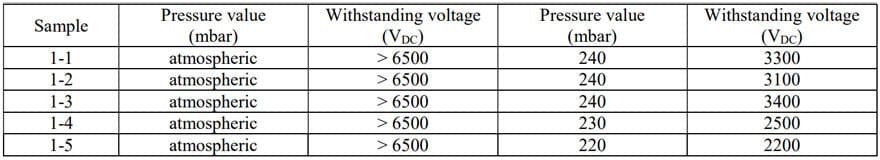
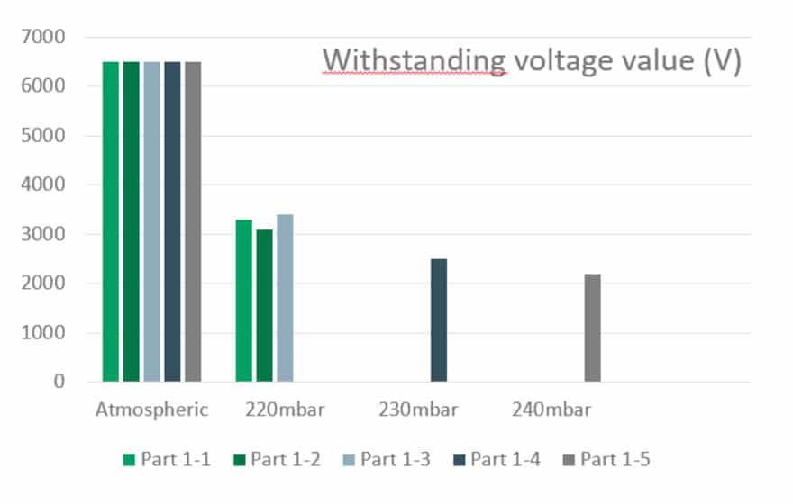
The difference of withstanding voltage is significant: from 6500 VDC at atmospheric pressure to 2200 VDC at lower pressure.

2 – Influence of glass barrier presence on withstanding values :

On the same parts as paragraph 1, some stacks of two chips have been manufactured, with glass line barrier (parts 2-1 to 2-5) vs no barrier stacks (parts 2-6 to 2-10), and all externally covered with a silicone varnish (aerosol deposition) to simulate customer potting (external leakage prevention). Only low pressure measurements have been performed.

Table 2: Withstanding voltage on 2220 varnished stacks with vs without glass barrier

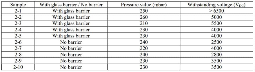
Withstanding voltage values are globally higher on stacks with glass barrier than without. Another run of trials has been performed on similar 2 chips stacks, with glass barrier or not, with no varnish, to try to localize the leakage when occurring, with insulation of the end terminations:

Table 3: Withstanding voltage on 2220 unvarnished stacks, end terminations covered, with vs without glass barrier

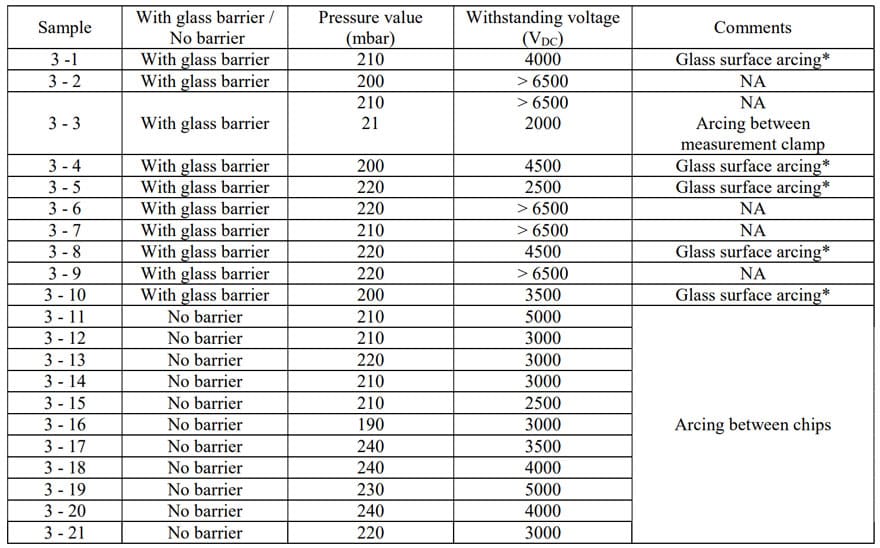
* the arcing on the surface of the glass occurs on the side of the stacks: the electrical arc goes around the glass barrier.

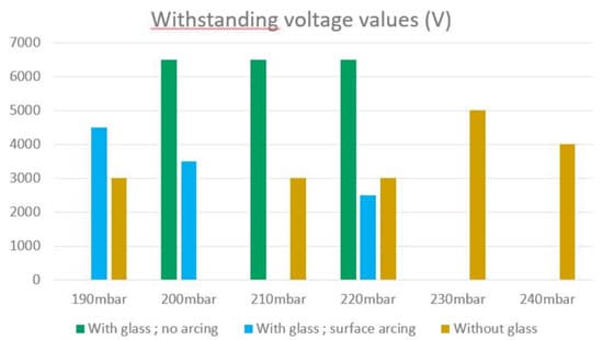
It is clear with this measurement configuration that glass barrier is efficient. The low pressure withstanding values of stacks with the glass barrier (parts 3-1 to 3-10, table 3) are similar to the reference ones at atmospheric pressure (parts 1-1 to 1-5, atmospheric values, table 1): no breakdown till maximum voltage delivered by test equipment (6500 VDC). On some parts, a leakage occurred at the surface of the glass (unvarnished surfaces on the sides of the stacks), which wouldn’t occur with an external potting.

Very low pressure measurement performed on part 3-3 (21mbar) also shows that it’s efficient for space conditions environment: the arcing occurred between the clamps and not on the parts. It means that the glass line deposed between the opposite poles acts as planned as a protective barrier, which improves breakdown voltage of the stack under low pressure.

CONCLUSION

Exxelia’s solution to manufacture reliable HV stacks useable in aeronautics and space conditions seems to work regarding presented results. It is a promising technology to decrease capacitor footprints in space applications. Exxelia is performing additional studies (including CSAM observations) to confirm this technology on various configurations (ceramics, sizes and thicknesses of the chips) and, also, on functional HV parts (with electrodes) before qualification and release to customers.

Related

Source: EPCI

Recent Posts

PCNS 2025 Final Program Announced!

31.7.2025
3

European Components Distribution (DMASS) Faces Continued Decline in Q2 2025

30.7.2025
5

Switched Capacitor Converter Explained

28.7.2025
12

Samsung Releases 1000V 1812 X7R 100nF MLCC for Electric Vehicles

28.7.2025
16

Samsung Electro-Mechanics Releases Molded MLCC Capacitors

28.7.2025
22

Researchers Demonstrated 200C Polymer Film Dielectric

28.7.2025
10

Researchers Demonstrated Zinc-Ion Based Photo-Supercapacitor

28.7.2025
9
Comparative display of a grain size and domain structure; b free energy; c P-E loops after high-entropy ceramics (HECs) and PGS design. source: Nature Communications  ISSN 2041-1723

Researchers Propose Novel MLCC Dielectric Design to Increase Energy Storage Capacity

24.7.2025
38

iNRCORE Releases New Range of 1KW HiRel Planar Transformers

24.7.2025
19

July 2025 Interconnect, Passives and Electromechanical Components Market Insights

23.7.2025
69

Upcoming Events

Sep 22
September 22 @ 13:00 - September 25 @ 15:15 EDT

Pre Cap Visual Inspection per Mil-Std-883 (TM 2017)

Sep 30
September 30 @ 12:00 - October 2 @ 14:00 EDT

MIL-Std-883 TM 2010

Oct 17
12:00 - 14:00 EDT

External Visual Inspection per MIL-STD-883 TM 2009

Oct 21
October 21 @ 12:00 - October 23 @ 14:15 EDT

Space and Military Standards for Hybrids and RF Microwave Modules

Nov 4
November 4 @ 12:00 - November 6 @ 14:15 EST

Wirebond Materials, Processes, Reliability and Testing

View Calendar

Popular Posts

  • Buck Converter Design and Calculation

    0 shares
    Share 0 Tweet 0
  • Boost Converter Design and Calculation

    0 shares
    Share 0 Tweet 0
  • Flyback Converter Design and Calculation

    0 shares
    Share 0 Tweet 0
  • LLC Resonant Converter Design and Calculation

    0 shares
    Share 0 Tweet 0
  • What is a Dielectric Constant and DF of Plastic Materials?

    4 shares
    Share 4 Tweet 0
  • Ripple Current and its Effects on the Performance of Capacitors

    3 shares
    Share 3 Tweet 0
  • Dual Active Bridge (DAB) Topology Explained

    0 shares
    Share 0 Tweet 0
  • How to Design an Inductor

    0 shares
    Share 0 Tweet 0
  • MLCC Case Sizes Standards Explained

    0 shares
    Share 0 Tweet 0
  • MLCC and Ceramic Capacitors

    0 shares
    Share 0 Tweet 0

Newsletter Subscription


Passive Components Blog

© EPCI - Leading Passive Components Educational and Information Site

  • Home
  • Privacy Policy
  • EPCI Membership & Advertisement
  • About

No Result
View All Result
  • Home
  • Knowledge Blog
  • Premium Suppliers

© EPCI - Leading Passive Components Educational and Information Site

This website uses cookies. By continuing to use this website you are giving consent to cookies being used. Visit our Privacy and Cookie Policy.
Go to mobile version