Passive Components Blog
No Result
View All Result
  • Home
  • NewsFilter
    • All
    • Aerospace & Defence
    • Antenna
    • Applications
    • Automotive
    • Capacitors
    • Circuit Protection Devices
    • electro-mechanical news
    • Filters
    • Fuses
    • Inductors
    • Industrial
    • Integrated Passives
    • inter-connect news
    • Market & Supply Chain
    • Market Insights
    • Medical
    • Modelling and Simulation
    • New Materials & Supply
    • New Technologies
    • Non-linear Passives
    • Oscillators
    • Passive Sensors News
    • Resistors
    • RF & Microwave
    • Telecommunication
    • Weekly Digest

    Smolteks CNF MIM Capacitor Break 1 µF/mm²

    Samsung Electro-Mechanics Releases 0201 X7T 1uF 6.3V MLCC for ADAS Applications

    Murata Announces 0402 Automotive Chip Ferrite Beads for V2X

    2025 Thick and Thin Film Resistor Networks Environment Overview

    Role of High-Q Ceramic Filters to Overcome GNSS Jamming

    Optimization of IoT for GEO NB-NTN Hybrid Connectivity

    TDK Releases Automotive Power-Over-Coax Inductor for Filters

    Advanced Conversion Announces Mass Production of 200C Film Capacitors

    VinaTech Supercapacitors: Enhancing Smart Meter Reliability and Efficiency

    Trending Tags

    • Ripple Current
    • RF
    • Leakage Current
    • Tantalum vs Ceramic
    • Snubber
    • Low ESR
    • Feedthrough
    • Derating
    • Dielectric Constant
    • New Products
    • Market Reports
  • VideoFilter
    • All
    • Antenna videos
    • Capacitor videos
    • Circuit Protection Video
    • Filter videos
    • Fuse videos
    • Inductor videos
    • Inter-Connect Video
    • Non-linear passives videos
    • Oscillator videos
    • Passive sensors videos
    • Resistor videos

    Understanding Switched Capacitor Converters

    Coupled Inductors Circuit Model and Examples of its Applications

    Inductor Resonances and its Impact to EMI

    Highly Reliable Flex Rigid PCBs, Würth Elektronik Webinar

    Causes of Oscillations in Flyback Converters

    How to design a 60W Flyback Transformer

    Modeling and Simulation of Leakage Inductance

    Power Inductor Considerations for AI High Power Computing – Vishay Video

    Coupled Inductors in Multiphase Boost Converters

    Trending Tags

    • Capacitors explained
    • Inductors explained
    • Resistors explained
    • Filters explained
    • Application Video Guidelines
    • EMC
    • New Products
    • Ripple Current
    • Simulation
    • Tantalum vs Ceramic
  • Knowledge Blog
  • Suppliers
    • Who is Who
  • Events
No Result
View All Result
Passive Components Blog
No Result
View All Result

New Method of Graphene Manufacturing at Scale

25.8.2020
Reading Time: 5 mins read
A A
Graphene Hall-effect Sensor; image source: Paragraf

Graphene Hall-effect Sensor; image source: Paragraf

There has long been a buzz around graphene, the one-atom-thick allotrope of carbon that boasts some extraordinary properties around thinness, flexibility, robustness and electrical conductivity. The hyperbole has seen graphene grandiosely described as a wonder material that is going to find transformative applications across the electronics sector.

Living up to that heightened sense of expectation has not proved easy, however. To date, graphene as a material has largely failed to deliver on its potential in electronic device applications, primarily because of how it is manufactured and processed. With that in mind, a pertinent question needs to be asked: will graphene ever deliver on the hype?

RelatedPosts

Smolteks CNF MIM Capacitor Break 1 µF/mm²

Samsung Electro-Mechanics Releases 0201 X7T 1uF 6.3V MLCC for ADAS Applications

Murata Announces 0402 Automotive Chip Ferrite Beads for V2X

To find an answer to that, we need to take a step back and look at some of the challenges of manufacturing graphene for use in the electronics sector.

There are quite a few companies making graphene powder (i.e. flakes of graphene) which is used as an adder material to improve the properties of polymers and cements. However, graphene electronic devices as products are still in their infancy because of many issues, one of which is a cost-effective method of producing sheets of graphene on wafers. There is also limited commercial knowledge about how to process these sheets into working, reliable electronic devices with good process yields.

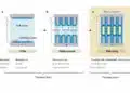
Most commercially produced graphene is either created by exfoliating graphite or forming the graphene onto a metal substrate — most commonly a copper foil. While exfoliating graphite produces good quality graphene, the graphene produced is typically very small area, multi-layered, non-homogeneous and non-customizable; therefore, it is not suitable for electronic devices other than at the R&D level.

Graphene grown on copper foil, meanwhile, needs to be transferred onto an electronics-compatible substrate after being synthesised, involving various wet and dry transfer processes that can affect how the graphene functions in an electronic device. It is also contaminated by the copper.

These challenges mean there has been a lack of contamination-free, transfer-free, large-area graphene available in the market, and adoption in mass-market electronics remains slow. New solutions are clearly required if graphene is to make its mark in the electronics sector.

Novel technique holds real promise

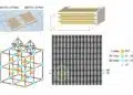
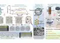
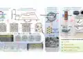
Paragraf has developed an innovative method of producing graphene at scale. This is achievable via a scalable and patented technology that enables manufacturing of large-area, high-quality graphene (currently up to 8” diameter).

The approach uses a modified deposition method that removes the need for the transfer processes commonly applied in most large area graphene synthesis methods. Therefore, the graphene can be produced in a uniform, single layer directly on a wide range of substrates, including silicon, silicon carbide, sapphire, gallium nitride, and other semiconductor-compatible substrates. It is also free from metallic contamination.

On the face of it, then, this scalable approach overcomes many of the challenges for developing graphene for electronics applications. The next step is to make the most of these advances by identifying suitable applications and bringing commercially viable products to market.

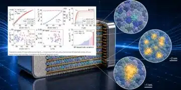
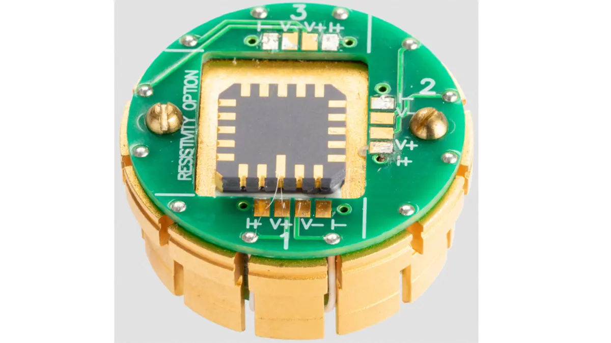
This process has already begun, with Paragraf’s scientists and engineers developing a new graphene-based Hall-Effect sensor. Existing Hall-Effect devices, made from silicon, are used primarily used for magnetic sensing. However, they have limitations in terms of sensitivity, accuracy and magnetic field range. Paragraf believes its graphene device will overcome many of these performance parameters.

So, let’s look at those claims in a bit more detail, starting with the specifics of why graphene, as a material, is so suitable for use in a Hall effect sensor. Crucially, graphene has a property called sheet carrier concentration: essentially the number of electrons available to move through the material carrying charge, which is very low. When configuring the material to interact with other electrical or magnetic fields, such as in a Hall effect sensor, this property directly translates to a very high level of sensitivity in the device. In real terms this can be 30 to 50 times more sensitive than a standard semiconductor such as silicon.

Also, importantly, graphene is a two-dimensional material, meaning it does not exhibit the same directional properties as thicker, or bulk materials. For Hall effect sensors this is particularly useful: one of the issues with traditional devices is the thickness of the sensing material, which causes the sensing layer to be three-dimensional. This causes field components that are not perpendicular to the sensing direction to also be sensed, and as a result, false signals are produced. This is known as the planar Hall effect. The lack of a planar Hall-Effect in Paragraf sensors is due to the inherent thinness of monolayer graphene, so these errors are removed, allowing for higher precision mapping of magnetic fields.

Also, graphene is very robust and does not suffer from the thermal impacts that conventional semiconductor devices do. This allows the sensor to work at more extreme temperatures, much higher and much lower than standard silicon semiconductor devices. They can be used in extreme cryogenic temperatures at conditions of less than -271 °C (1.8 K) and currently up to 80 °C (353 K), meaning they can be used in superconducting environments while remaining highly sensitive. As well as being resistant to thermal shock, no electrostatic discharge protection is required, and the sensors can be plugged straight into the mains (220V) without any adverse effects occurring. This makes the sensors easier to handle in industrial environments.

The graphene-based Hall-Effect sensors also have very low power dissipation — of the order of picowatts (pW) with nanoamperes (nA) drive current – so they will not heat cryogenic environments and will save energy compared to other Hall-Effect sensors.

Paragraf is currently offering its graphene Hall-effect sensor in low volumes for its use in a wide range of magnetic measurement applications ahead of a full commercial launch later this year. The sensors are priced to reflect the opportunity to gain first access to this new and disruptive technology and are supplied as part of a collaborative package, which is costed on an application-by-application basis depending on the required level of customization and support from Paragraf.

Field testing provides validation

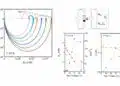
The technical characteristics of the Paragraf sensor have been proven during field tests with several partners. For instance, Paragraf is working with the Magnetic Measurement Laboratory of the European Organization for Nuclear Research (CERN), which has tested sensors to see if they could accurately map the magnetic fields in electromagnets used within CERN’s unique set up. The field tests show definitively that Paragraf’s sensor has a negligible planar Hall Effect and therefore only measures field components along the desired axis of measurement. CERN is looking to build a stacked mapping system of Hall Effect sensors that can provide very accurate magnetic field measurements using Paragraf’s Hall Effect sensors.

Paragraf has also been working with the National Physical Laboratory (NPL) to investigate the suitability of sensors in extremely harsh environments and with Queen Mary University of London to study the potential of graphene to replace indium tin oxide in electronic devices.

The sensors could theoretically be embedded into aircraft engines for the continuous monitoring of faults in real-time. Also, once the testing work with the NPL is complete, and the sensor is shown to be capable of operating in harsh radiation environments, applications could include use as positional sensors within nuclear-decommissioning robots and space satellites.

Related

Source: EE Times

Recent Posts

H2-Assisted Thermal Treatment of Electrode Materials Increases Supercapacitors Energy Density

13.5.2025
14

Researchers Present Hybrid Supercapacitor Zn-Ion Microcapacitors

12.5.2025
46

Murata and NIMS Built New Database of Dielectric Material Properties

5.5.2025
90

3D Printing of Passive Components from Manufacturer Perspective

26.4.2025
53

Hybrid Electrochemical Electrolytic Capacitor Provides High Frequency and High Capacitance Performance

25.4.2025
75

Supercapacitor Separator with High Ionic Conductivity Enables Line-Filter Applications at High Power

21.3.2025
52

Interlacing Strain Engineering Boost Energy Density of MLCCs

12.2.2025
85

Researchers Developed BaTiO3 based MLCC Material with High Energy Density at High Temperature Range

21.1.2025
111
A film a few atoms thick of non-crystalline niobium phosphide conducts better through the surface to make the material, as a whole, a better conductor. | Il-Kwon Oh / Asir Khan

Researchers Developed High Conductive Nanowires

20.1.2025
60

CNF-MIM Capacitors Benefits vs Deep Trench Capacitors

9.1.2025
137

Upcoming Events

Jun 24
16:00 - 17:00 CEST

Limitations of PSFB converters and improvements by a variable inductor ft. Sam Ben-Yaakov

Jun 24
17:00 - 18:00 CEST

Ultra-Compact and Efficient Switched-Capacitor Power Converters

Jul 23
13:00 - 14:00 CEST

PCB design for a Smartwatch

View Calendar

Popular Posts

  • Buck Converter Design and Calculation

    0 shares
    Share 0 Tweet 0
  • Boost Converter Design and Calculation

    0 shares
    Share 0 Tweet 0
  • Flyback Converter Design and Calculation

    0 shares
    Share 0 Tweet 0
  • What is a Dielectric Constant and DF of Plastic Materials?

    4 shares
    Share 4 Tweet 0
  • LLC Resonant Converter Design and Calculation

    0 shares
    Share 0 Tweet 0
  • Ripple Current and its Effects on the Performance of Capacitors

    3 shares
    Share 3 Tweet 0
  • How to Design an Inductor

    0 shares
    Share 0 Tweet 0
  • Dual Active Bridge (DAB) Topology Explained

    0 shares
    Share 0 Tweet 0
  • SEPIC Converter Design and Calculation

    0 shares
    Share 0 Tweet 0
  • Why Low ESR Matters in Capacitor Design

    0 shares
    Share 0 Tweet 0

Newsletter Subscription


Passive Components Blog

© EPCI - Leading Passive Components Educational and Information Site

  • Home
  • Privacy Policy
  • EPCI Membership & Advertisement
  • About

No Result
View All Result
  • Home
  • Knowledge Blog
  • Premium Suppliers

© EPCI - Leading Passive Components Educational and Information Site

This website uses cookies. By continuing to use this website you are giving consent to cookies being used. Visit our Privacy and Cookie Policy.
Go to mobile version