Source: Nature Journal abstract
Negative capacitance is a newly discovered state of ferroelectric materials that holds promise for electronics applications by exploiting a region of thermodynamic space that is normally not accessible.
Although existing reports of negative capacitance substantiate the importance of this phenomenon, they have focused on its macroscale manifestation. These manifestations demonstrate possible uses of steady-state negative capacitance—for example, enhancing the capacitance of a ferroelectric–dielectric heterostructure or improving the subthreshold swing of a transistor.
Yet they constitute only indirect measurements of the local state of negative capacitance in which the ferroelectric resides. Spatial mapping of this phenomenon would help its understanding at a microscopic scale and also help to achieve optimal design of devices with potential technological applications.
Here we demonstrate a direct measurement of steady-state negative capacitance in a ferroelectric–dielectric heterostructure. We use electron microscopy complemented by phase-field and first-principles-based (second-principles) simulations in SrTiO3/PbTiO3 superlattices to directly determine, with atomic resolution, the local regions in the ferroelectric material where a state of negative capacitance is stabilized. Simultaneous vector mapping of atomic displacements (related to a complex pattern in the polarization field), in conjunction with reconstruction of the local electric field, identify the negative capacitance regions as those with higher energy density and larger polarizability: the domain walls where the polarization is suppressed.
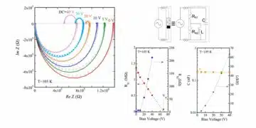
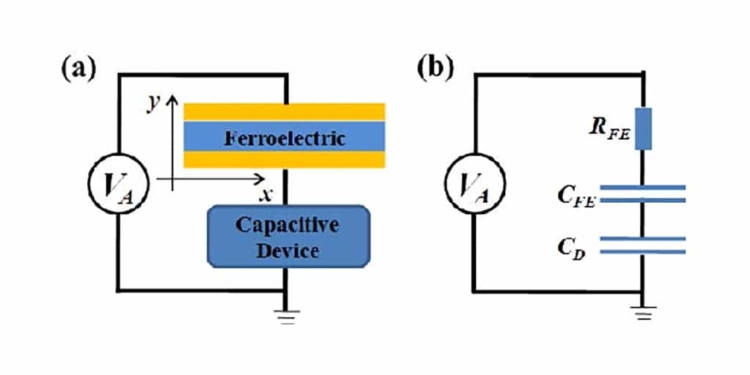
featured image: Schematic of a metal-ferroelectric-metal capacitor connected in series with a normal capacitive device and (b) the equivalent circuit of (a) image credit: Zhengyong Zhu in his IEEE article.
full article can be purchased at Nature Journal link here.


