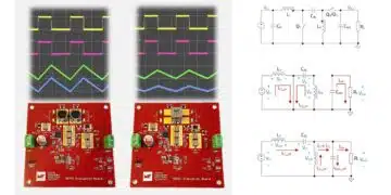
source: EDN article
The “GaN revolution” may re-define a whole component market and passive components selection guidelines. Have a look at the latest EDN article by TI on the comparison of 48V to 1V conventional silicon and GaN power converter design. One can note the significant change in passive component needs. T.Zednicek EPCI
Alberto Doronzo, Applications Power Engineer, High Voltage Power Solutions, Texas Instruments -October 22, 2016. 48 V to point-of-load (PoL) conversion is common in numerous markets, including telecommunications, industrial, aerospace and increasingly server environments. The prevalent system solution is a two-stage conversion from 48 V to an intermediate bus (9 V to 12 V) and then to PoL, typically 0.8 V to 3.3 V.
Data center operators are particularly interested in single-stage 48-V to low-voltage DC/DC conversion and its associated efficiency gains, because data centers may consume as much as 140 TWh of power usage in the U.S. yearly by 2020 [1], or about 3.5 percent [2] of overall U.S. usage. The PoL in the application discussed in this article includes general-purpose and application-specific processors, field-programmable gate arrays (FPGAs) and application-specific integrated circuits (ASICs).
While the limitations of silicon-based converters force a two-stage solution, new gallium nitride (GaN) devices enable single-stage conversion. Two key design requirements are efficient power conversion and ultra-fast load transient response of the ASIC/processor core rails.
GaN’s advantages are strongly evident during single-stage conversion, with higher efficiency and smaller size than traditional solutions, while simultaneously reducing bill of materials (BOM) count and systems cost. In this article, I will discuss the design of a 48-V to 1.0-V PoL 50-A converter using a GaN half-bridge module and a high-performance controller for the single-stage topology, achieving efficiency exceeding 90 percent.
Introduction
GaN devices provide stronger performance and more ideal switching characteristics compared to silicon. GaN enables more efficient and smaller power systems. However, the greatest benefit of GaN does not come from a direct silicon substitution in an existing topology; the key to using GaN is to identify applications and converter topologies that specifically harness GaN’s advantages. With GaN’s low switching loss and zero reverse recovery, hard-switched half-bridge topologies show noticeable performance improvements. One of the strongest application areas for GaN is in the 48-V input converter space, targeting telecom and industrial customers as well as aerospace and server applications.
In 48-V telecommunications and server applications, there is strong demand for conversion down to PoL in order to power processing-intensive cores like microprocessors, FPGAs and ASICs. Traditionally, the conversion from 48 V down to PoL uses a two-stage approach. This entails a brick-type bus converter performing an isolated conversion between 48 V and an intermediate voltage such as 12 V or 9 V using a hard-switched half-bridge or full-bridge topology, or a resonant topology such as inductor-inductor-capacitor (LLC). Next, a multiphase buck converter converts down to PoL at up to 200 A, while handling the transient response requirements of a highly dynamic digital load.
The traditional solution’s beginning-to-end efficiency is a product of the two individual stages. With the first stage peak efficiency of 96 percent and the multiphase buck stage peak efficiency close to 92 percent, the total efficiency is only 88 percent (Figure 1) at frequency ranges between 100 to 200 kHz. The two-stage solution also has a larger board-area footprint.

Figure 1: Texas Instruments GaN solution versus a silicon traditional solution.
A single-stage approach would improve efficiency and reduce board area. While this has been the desired target for a long time, silicon-based designs have not demonstrated a compelling solution. GaN enables an elegant new topology that offers PoL-level transient response from a single, efficient 48-V to PoL conversion stage, while running at higher frequencies close to 600 kHz, further aiding size reduction.
Converter topology
An isolated half-bridge with a current-doubler output topology is extremely advantageous for this type of application, as shown in Figure 1. In this topology, a GaN half-bridge (using the LMG5200) connects to the transformer, which is referenced to a split capacitor network to provide voltage balancing.
The secondary side connects in a current-doubler synchronous rectifier, which enables better heat distribution, a simpler transformer design and the advantage of foregoing high-side switches, as both are ground referenced. Since the charging current of the capacitor is the sum of the two inductor currents, which are 180º out of phase, the output voltage ripple is halved
Figure 2 shows synchronous rectifiers instead of diodes. The average current through these rectifiers can reach 25 A, which a diode would not be capable of sustaining in an application Note that the rectifiers will be operating in continuous conduction mode and will be subject to reverse recovery; therefore, the preferred choice is GaN FETs, as they present the advantage of zero recovery loss. Alternatively, using silicon FETs requires very tight dead-time control. Figure 3 illustrates the operation of the current-doubler converter.


High-performance control
The current and voltage behavior for this topology resembles a two-phase buck converter, for which controllers are available and need little modification. The fast transient response requirement makes the TPS53632G a possible candidate for this application: using the D-CAP+™ controller with valley current mode and constant on-time control, the load transient response is extremely accurate and fast, while being able to switch up to 1 MHz, with a finely adjustable output (7 bits) voltage though the I2C bus.
Hardware design
There are several advantages to the single-stage architecture when using this topology. First and foremost is the reduced size (by ~75 percent) and number of components (by ~40 percent) due to the single stage and the higher switching frequency that allows exclusive use of a ceramic capacitor and small magnetics. This reduced size is achieved by using a GaN-enabled hard-switched topology. Second, there is a power-conversion efficiency gain due to the reduction in stages and the simplification of the transformer, which is designed with a low turn ratio of 5 to 1, and be integrated into a 10-layer printed circuit board (PCB). The simplified transformer further reduces assembly complexity, cost and height profile. The active power-conversion area for a 50-A solution measures 1.45 by 0.75 inches, which is nearly a sixteenth brick (1.3 by 0.9 inches), with a peak efficiency of 90-92 percent, as shown in Table 1.
Table 1: 48-V to PoL board specifications.

Despite the fact that the maximum voltage seen by the secondary FETs is below 10 V, I used 30-V GaN FETs, which was the lowest voltage available at the time of this writing. You could certainly use a lower-volt GaN FET, if available. Also, by bringing the 48 V closer to the load, the distribution copper losses of the system drop by a factor of (48 V/12 V)2 = 16.
Figure 4 shows the measured efficiency in the converter across the load, with varying input voltages. This is a full system efficiency plot, which includes controller and driving losses. It is noteworthy that the full-load 50-A efficiency is essentially the same for 48-V and 60-V inputs, as well as for 36-V and 75-V inputs.

Figure 4: Efficiency versus load and input voltage.
Peak efficiency occurs at a lower VIN – 91.5 percent at 36 V – but the high output current causes severe copper losses, which are clearly visible on the thermal images shown in Figure 5.

Figure 5: The secondary side getting warm because of the high current in traces.

Figure 6: GaN 600-kHz 48-V to PoL solution versus a silicon state-of-the-art solution.
The two-state silicon-based solution in this example uses a 50-V to 12-V unregulated 600-W quarter-brick converter running at 190 kHz, with 97.1 percent peak efficiency. This first stage is followed by a 12-V to 1-V 50-A eighth-brick converter. Running the second stage at 200 kHz and 600 kHz for better comparison resulted in peak efficiencies of 93.5 percent and 87 percent, respectively.
The GaN solution at 600 kHz shows a higher and flatter efficiency curve compared to an equivalent silicon-based solution running at 200 kHz.
Dynamic performance
It is possible to achieve ultra-fast load transient response in the PoL application by using the analog D-CAP+ controller and GaN to switch at a frequency higher than what is possible with silicon. A 10-A step, as shown in Figure 7 and Figure 8 for load insertion and release, causes a mere 25- to 30-mV perturbation on the output voltage while using small ceramic capacitors. Because the D-CAP+ controller is extremely fast, it is possible to reduce the number of output capacitors compared to what would be required with other control modes.

Figure 7: Loading step response.

Figure 8: Unloading step response.
Conclusion
When implementing new GaN-enabled solutions, the advantages extend beyond the simple figure-of-merit improvements shown in Figure 1.
As exemplified in this conversion to PoL application, there are space and power savings external to the power block, which when coupled with efficiency and component-related cost-reduction improvements far offset the higher cost of GaN and bring significant advantages to the whole system.
These are the successes that will pave the way toward widespread adoption of GaN in power electronics and result in significant efficiency improvements in cloud infrastructure equipment and data centers.


