


This paper 3D printing of passive electronic components from the perspective of a components manufacturer was presented by Johann Pichler, TDK, Austria during the 5th Space Passive Component Days (SPCD), an International Symposium held from October 15th to 18th, 2024, at ESA/ESTEC in Noordwijk, the Netherlands. Published under permission from ESA SPCD organizers.
Introduction:
The article explores the transformative potential of 3D printing technologies in the manufacturing of passive electronic components, particularly from the perspective of a components manufacturer.
While traditional methods excel in high-volume, cost-efficient production, they face limitations in design flexibility, development cycles, and customization.
The research delves into how recent advancements in materials and 3D printing techniques could address these challenges, enabling faster time-to-market, low-volume, and application-specific component designs.
Key Points:
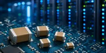
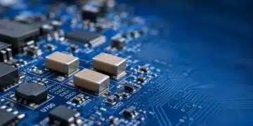
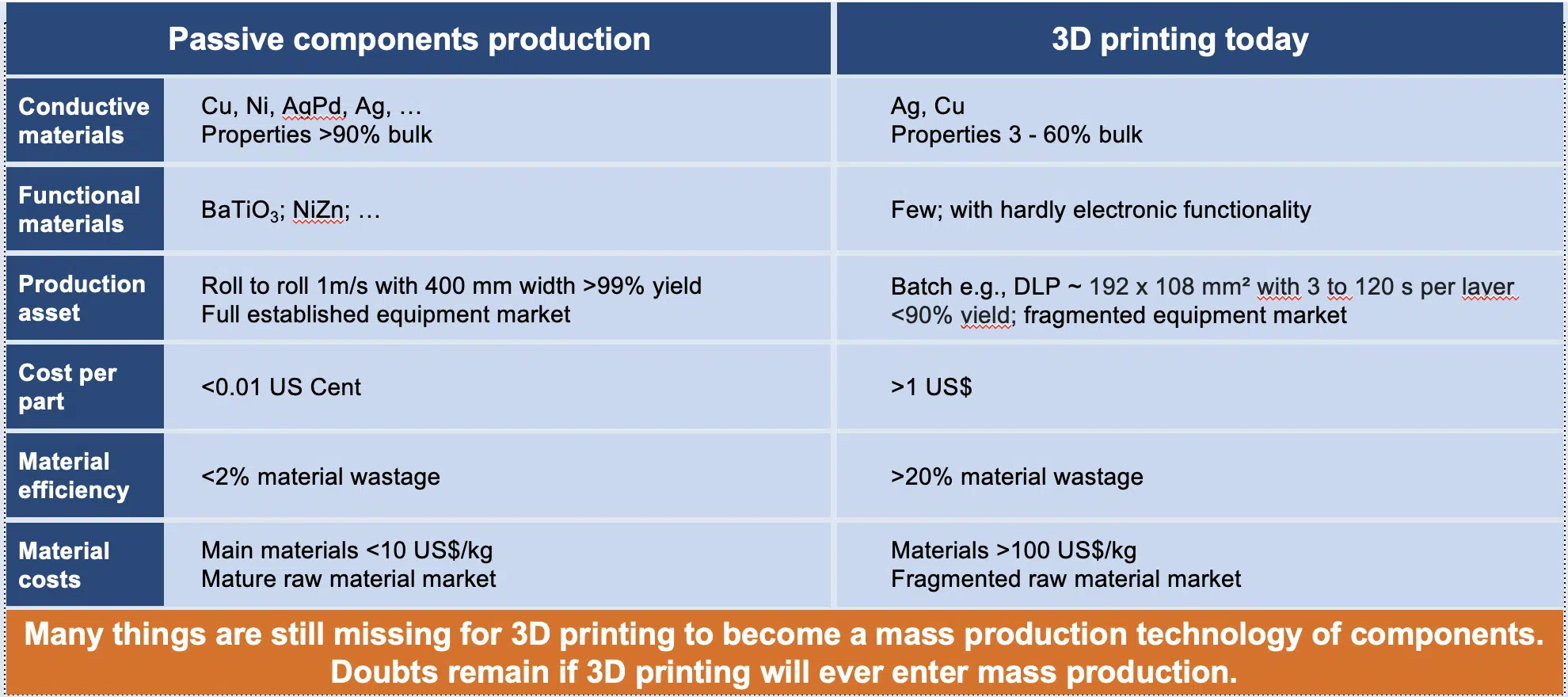
- Current Manufacturing Limitations: Traditional manufacturing (e.g., MLCC) is optimized for mass production but lacks flexibility for complex geometries and custom designs.
- 3D Printing Potential: Offers design freedom, rapid prototyping, and the ability to integrate structural and functional elements.
- Challenges: Includes slow printing speeds, material compatibility issues, and post-processing requirements.
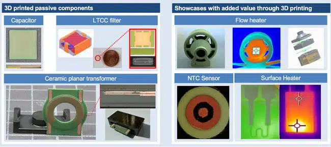
- Application Examples: Demonstrates prototypes like microfluidic devices and MEMS packages showcasing 3D printing’s integrated capabilities.
- Future Outlook: 3D printing is unlikely to replace traditional methods but holds promise for niche, high-performance markets.
Extended Summary:
The article begins by underscoring the critical role of passive electronic components in modern devices. It details the traditional manufacturing process of Multi-Layer Ceramic Capacitors (MLCCs), which involves rigorous methods such as screen printing, stacking, cutting, and sintering. These processes, while efficient for mass production, are product-specific, leading to inflexibility and high costs for custom, low-volume products.
The discussion transitions to the limitations inherent in current manufacturing techniques—narrow process windows, tooling constraints, and lengthy development cycles. These challenges highlight the potential for 3D printing technologies to revolutionize the field. Unlike conventional methods, 3D printing allows for the creation of complex geometries without the need for specialized tooling. It enables rapid prototyping, on-demand production, and the possibility of integrating multiple functions within a single component.
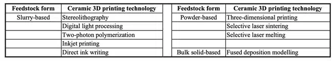
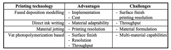
The article categorizes 3D printing technologies into several types, such as material extrusion, binder jetting, and vat photopolymerization, explaining their respective applications in fabricating ceramic structures. Despite its advantages, 3D printing faces challenges like slow production speeds, material property mismatches, and intricate post-processing requirements, especially for multi-material printing.
Selected application examples demonstrate the practical benefits of 3D printing. A microfluidic device illustrates how complex internal channels and integrated heating elements can be produced efficiently. Another example highlights a hermetic package for a MEMS device, showcasing the design freedom and functional integration achievable through 3D printing.
Conclusions:
The article concludes that while 3D printing will not replace traditional mass-production technologies for passive electronic components, it offers significant advantages for specific applications.
These include the production of free-form components and highly integrated systems combining structural and functional elements. The technology’s true value lies in applications where design flexibility, rapid development, and functional integration outweigh the cost implications. Continued advancements in multi-material 3D printing and material science will be key to unlocking its full potential in electronics manufacturing.