


Electrostatic capacitors dominates the market among the other capacitor technologies. The article provides introduction into construction of electrostatic capacitors, such as ceramic, film, paper technologies.
Assembly styles, termination techniques or metallization processes are explained including impact to the basic paramters. Specifically described is film capacitors’ self-healing process and how this can be impacted by selection of materials and manufacturing process.
Key Takeaways
- Electrostatic capacitors dominate the market, with various technologies like ceramic and film influencing their design.
- The construction of electrostatic capacitors includes methods like stacking and winding to enhance capacitance.
- Key parameters such as electrode spacing and dielectric materials affect the capacitors’ performance and voltage capabilities.
- Metallization processes replace traditional foils with thinner layers, improving capacitance and self-healing capabilities.
- Pulse and voltage applications require careful management of current densities to prevent capacitor failure.
Lets start with a general consideration of electrostatic capacitor designs. There are some design solutions and “tricks” to reinforce capacitor features to meet specific application requirements such as higher power, higher safety robustness.
Construction & Assembly
The search for capacitance in small volumes has created a number of different solutions, each with its advantages and drawbacks. We shall try in this chapter to describe both methods and problems of achieving large C/V ratios. Further details may be added in specific material sections.
The latter part of this chapter deals with some general construction questions.
Stacking
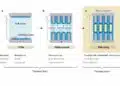
Suppose we have 6 capacitor elements consisting of 2×6 electrodes organized as in Figure 1. We understand that spread in one plane and connected together they will result in a total capacitance 6C. Generally, N electrodes give the capacitance N/2 C.
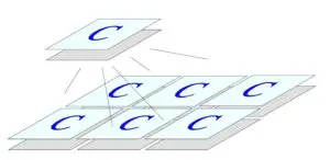
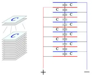
Instead, if we stack them according to Figure 2. capacitance will be developed between every electrode with different polarity which here results in 12-1 = 11 elements connected in parallel. Ctot = 11C. In general N electrodes give Ctot = (N-1)C. The higher N the closer to a doubling of the one-plane capacitance with the stacked capacitor type.
Winding
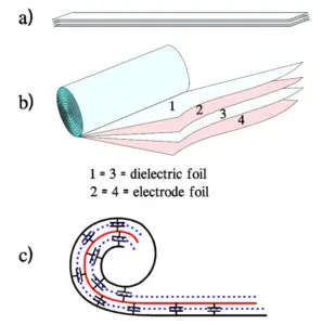
If we spread two metal foils separated by two insulating foils as shown in Figure C3. (a) and wind the foil package to a winding (b) the capacitance is doubled in the same way as with the stacked type. The electrodes will be capacitive in two directions (c).
Terminations

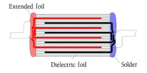
The termination to the electrodes is performed either with one or several so called inserting tabs (for example tinned copper foils) which connect the electrodes with the terminals). Or one can let the electrode foils extend from the winding and bend them against the winding end (extended foil construction) where they are soldered or welded to the terminal leads (Figure 4). A remark concerning inserted tabs. Should the working voltage be low and the capacitor oil impregnated the tabs have to be welded to the electrode foils if we shall avoid open circuit risks. In electrolytics aluminum tabs have to be welded – preferably cold welded – to the foils because of the corrosion risk.
Minimized electrode spacing
In accordance with the formula C = ε x A/d we improve capacitance by the degree to which we decrease the electrode spacing, d. Improved technology has permitted manufacture of certain plastic films down to less than 0.5 μm (0.02 mils) in thickness. The so called wet method used in ceramic manufacturing has lead to thicknesses less than 15 μm (0.6 mils) and a developed dry method based on a plastic film conveyor or carrier has reduced the dielectric thickness even further, to less than 5 μm (0.2 mils).
To the thinnest dielectric of different material groups corresponds the lowest rated voltage capability. We have to comply with that thickness irrespective of the working voltage. If we, for example, need 6 V DC the nearest working voltage might be 10 V. But only in ceramic. Plastic films stop at 16 V, porcelain and paper at 100 V, mica at 125 and glass at 250 V DC.
The dielectric withstanding voltage
puts another limit to the thinness of a dielectric. The higher the working voltage, the thicker the dielectric must be. But if the thickness increases 5 times, the capacitance decreases to 1/5 or for the same capacitance, the volume of the part must be 5 times greater. Hence high voltage capacitors always will be bulky.
Higher dielectric constant, εr
Plastic and paper foils have a relative dielectric constant around 3. If we change to ceramics it’s possible to increase the εr by several thousands. But in different ways we loose the quality characteristics significant for other materials, such as, polymers. In the different dielectric material groups we will account for the typical characteristics.
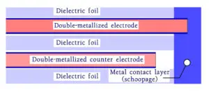
Metallization
The so called foil capacitor has electrodes consisting of aluminum, 5…10 μm (0.2…0.4 mils) thick. Every turn in a capacitor winding adds at least 2×5 μm (2×0.2 mils) metal foil + dielectric which means that the electrodes in a low voltage capacitor accounts for the greater part of the volume. By means of metal vaporization in vacuum – the so called metallization – the foil electrodes are replaced with a very thin metal layer on one side of the dielectric foils. On metallized paper foils (MP) the metal usually is zinc (Zn). Its sensitivity to oxidation and corrosion in moisture is overcome by the necessary impregnation of the paper winding. In plastic foil capacitors generally no impregnation is needed and here one has been obliged to use aluminum (Al) because of its better chemical resistance. Now, however, some corrosion resistant alloys are introduced with the same advantageous characteristics as zinc.
The metallization layer is thinner than 0.1 μm with typical values around 0.02 to 0.05 μm (0.8 to 2 microinches). The specific capacitance gain is considerable.
The vaporized metal is at a high temperature and therefore the dielectric foils have to be cooled down significantly in order not to be damaged. This is achieved by letting the foil pass over drums cooled down to -30°C in the metallization chamber. The surface texture of the film certainly is changed but otherwise it is preserved intact. Some non-polar plastics like polypropylene (PP) initially suffered from problems with the adhesion to the metal. Currently manufacturers have learned to pre-treat the plastic surface properly.
In some constructions the metal foil electrodes are re-placed by double-sided metallized plastic foils, usually polyester. The design has a number of advantages, not only compared to metal foil electrodes.
Advantages to double-sided metallizing.
- Plastic foils can be made thinner than metal foils.
- TC of certain materials is unfavorably affected by the mechanical forces in metal foils.
- Metal foils also may produce capacitance hysteresis at temperature changes.
- The double metallizing increases the pulse load capability significantly compared to single metallized designs.
- Finally the metallization permits self-healing breakdowns. Because of reduced charge current densities the metallization could be correspondingly thinner, thus reducing the required self-healing energy.
Drawback.
- The voltage rise time/pulse capability is not of the same magnitude as that of metal foil designs.
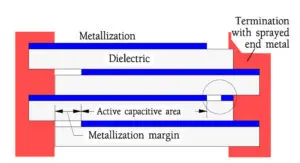
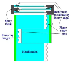
Termination
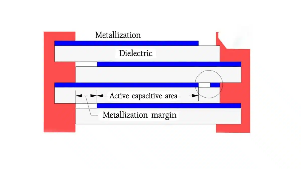
The metallized layer is connected to the terminals by means of a sprayed metal compound applied on the winding or stack ends. The process sometimes is called schooping. By shifting the foils alternately and terminating their metallization a little bit from the edge a short circuiting to the opposite terminal is prevented (Figure 6). The figure also shows the active capacitive area which for obvious reasons is maximized. It is done at the expense of the metallizing margins. The balance between security against short circuit and as small margins as possible requires great skillfulness and manufacturing accuracy. Margins of 0.2…0.3 mm (8…12 mils) are regarded as risky with respect to the IR quality while a margin of 1 mm (40 mils) eliminates these risks. Some manufacturers metallize the whole width of the foil and make a laser cut along one edge – encircled area in Figure C6 – and achieve in this way a more controlled metallizing margin simultaneously as they obstruct forbidden penetration of the end spray metal. Note however that the figure following, for reasons of emphasis, is far from being to scale.
The termination quality varies from one manufacturer to another. Therefore it is of vital importance by simple means to be able to detect parts with fault terminations. The utilization of ESR measurements taken at the resonance frequency of the capacitor in order to evaluate the contact quality in metallized film capacitors successfully has been used by number of companies in practice. For example, if the test specimens have been subjected to a heat treatment the differences in ESR quality appear most distinct.
Voltage rise time / current pulse
Because the metallization is very thin and its connection with the end spray metal is a surface contact and not a bulk metal layer the current into the electrodes must be limited. Above all, it is pulse loads that are the problem. When the charges rush in from the ends they successively are bound to the electrodes. Hence the highest current densities are at the electrode edges. Exactly here there is a risk that the ESR of the contact junction causes a local rise in energy development that a weak spot in the metallization is burnt off. This burning reduces the remaining current area. The next current pulse will result in an incrementally higher current density over the remaining area, the next weakest spot is burned away, and so on. Eventually the part fails open. The current, which can be described as dQ/dt, depends with start from the formula [1] of the voltage differential quotient as
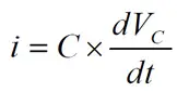
…….. [1]
Therefore metallized film capacitors must not be subjected to more than the limited voltage differential quotients that the manufacturer states in his data sheets. Here are some examples of stated maximum values:
- standard capacitors 5…20 V/μs.
- pulse application types 100…2500 V/μs.
In pulse applications the weakest link in the current paths is reinforced, i.e. the joints between end spray metal and the metallized layer. Among other means, reinforcement is achieved through choice of a suitable end spray metal, by reinforcement of the metallization along the contact edge as shown in Figure 7. and more and more often by contact favorable metallizing alloys. Some stacked types (see next passage) with Al metallization have an end spray of aluminum. Also the double-metallized electrodes as already described under 2.1.6 represent a considerable improvement of the pulse capability.
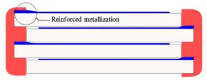
A further improvement of the pulse strength is a combination of the reinforced metallization and a wavy cut in the foils as shown in Figure 8. The wavy cut enlarges the contact area which means a lower contact resistance and a subsequent higher pulse strength.
Metallized stacked capacitors
If a winding should experience repeated voltage or current pulses that start burning off marginal parts of the contact edge it will, according to our previous discussion, end up with a complete open circuit. If instead of a winding we had had a stack of metallized foil parts (stacked type) an element with a degraded contact should have been eliminated. But the current into the remaining elements won’t be changed because one element is burnt off. The capacitor will work equally well at repeated pulses (with somewhat reduced total capacitance). The safety margins against contact edges being burnt off can, for stacked capacitors, be reduced which means the pulse rating can be kept higher in comparison to the rating for a corresponding wound design.
The manufacturing is done so that one winds a so called mother capacitor on an enormous wheel. The mother capacitor is metal sprayed (schooped) from the sides and then segmented to form capacitors which are finally finished in the usual way. The large diameter of the mother capacitor makes every little sector piece (part capacitor) nearly planar. When the saw cuts through the mother capacitor the plastic melts in a surface region and fragments of the metallization are dispersed in the locally melted plastic so that a sufficient insulation distance is created between the electrodes. In another method of manufacturing one winds on a flat plate and cuts the large plane parts of the winding into suitable elements.
Frequently Asked Questions about Electrostatic Capacitors
Electrostatic capacitors are passive components that store energy in an electric field. They dominate the capacitor market and include technologies such as ceramic, film, and paper capacitors.
They are built using stacking or winding methods, with electrodes separated by dielectric materials. Termination techniques include inserted tabs or extended foil connections.
Key parameters include electrode spacing, dielectric thickness, dielectric constant, and metallization processes. These affect capacitance, voltage rating, and reliability.