


In this webinar Würth Elektronik “How does your PCB layout influence the costs in PCB manufacturing?”
For example, did you know that switching to a slightly smaller drill bit can cause a much higher PCB price in some circumstances?
The webinar will be of interest to developers, purchasing and management. Get insight into how PCB design is linked to the implications for PCB manufacturing and the costs involved.
We provide guidance on the general cost structure of a PCB with a view to its layout and geometry. In this webinar you will learn more about
- PCB size, shape and panel layout
- Material selection and cost
- Layer stack and via design
- Mechanical processing
How PCB Layout Influences Costs in PCB Manufacturing
Introduction
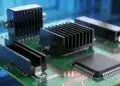
Printed Circuit Boards (PCBs) are at the heart of modern electronic devices. Understanding how PCB layout influences manufacturing costs is crucial for developers, purchasing managers, and decision-makers. This presentation delves into key factors that impact PCB costs, referencing insights from Würth Elektronik’s webinar.
1. PCB Size and Panel Layout
- Panel Utilization: Smaller PCBs allow more units per panel, reducing cost per PCB.
- Yield Considerations: Higher panel utilization mitigates yield loss from defects.
- Sustainability: Smaller PCBs reduce material usage, benefiting the environment.
2. Material Selection and Cost Factors
- Copper Pricing: Fluctuations in copper prices significantly impact PCB costs.
- Material Efficiency: Optimal copper thickness and material usage can reduce expenses.
- Surface Finishes: Choices like ENIG, HASL, and OSP affect cost based on durability and application.
3. Layer Stack-Up and Via Design
- Standard vs. Custom Stack-Ups: Custom configurations increase costs due to material and processing complexities.
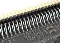
- Via Types: Microvias, buried vias, and through-hole vias influence drilling costs and board reliability.
- Controlled Impedance: Requires precise stack-up design and testing, adding to production costs.
4. Mechanical Processing
- Drilling: Smaller drill bits are costlier due to tool wear, slower processing, and reduced panel stacking capabilities.
- Routing vs. V-Scoring: V-scoring is more cost-effective for rectangular PCBs, while complex shapes require costly routing.
5. Enhanced Technologies and Cost Drivers
- Edge Plating & Castellated Holes: Additional plating steps increase costs.
- Colored Solder Masks: Non-standard colors require extra processing, elevating expenses.
- Special Requests: Custom packaging, labeling, or tests add to manufacturing time and costs.
6. Cost-Reduction Strategies
- Optimized Panel Design: Maximize PCB count per panel to distribute costs efficiently.
- Material Choices: Balance performance needs with cost-effective materials.
- Design Rule Compliance: Adhering to manufacturer’s DRC reduces errors and rework.
- Reduce Unnecessary Specifications: Avoid overengineering, such as requesting IPC Class 3 when Class 2 suffices.
Conclusion
Effective PCB cost management requires a holistic approach—considering size, materials, stack-up configurations, and mechanical processing. Collaboration with manufacturing partners like Würth Elektronik can optimize layouts, materials, and processes to achieve cost-efficient outcomes without compromising quality.