Passive Components Blog
No Result
View All Result
  • Home
  • NewsFilter
    • All
    • Aerospace & Defence
    • Antenna
    • Applications
    • Automotive
    • Capacitors
    • Circuit Protection Devices
    • electro-mechanical news
    • Filters
    • Fuses
    • Inductors
    • Industrial
    • Integrated Passives
    • inter-connect news
    • Market & Supply Chain
    • Market Insights
    • Medical
    • Modelling and Simulation
    • New Materials & Supply
    • New Technologies
    • Non-linear Passives
    • Oscillators
    • Passive Sensors News
    • Resistors
    • RF & Microwave
    • Telecommunication
    • Weekly Digest

    Skeleton Supercapacitor Achieves UL‑certified 3,500 A Peak Current for AI Data Centers

    Bourns Planar Transformers for SiC and GaN Gate Driver Isolation

    100 V Hybrid Polymer Capacitor from VINA Enesol Targets 48–72 V Power Platforms

    Panasonic Releases Relays for IEC 62955 Compliant Single‑Phase EV Wallboxes

    KYOCERA AVX Releases NTN Antenna Selection Guide Brochure

    Coilcraft Releases 0402 Ferrite-Core Wirewound Chip Inductors for RF and EMI Control

    DigiKey Releases Season Two of Sustainable Futures Series

    Using a Virtual Anode Thermal Model to Evaluate Miniaturization Risk in Tantalum Capacitors

    Bourns Introduced High-Current Coupled Inductor for 48 V Hybrid and IBC Converters

    Trending Tags

    • Ripple Current
    • RF
    • Leakage Current
    • Tantalum vs Ceramic
    • Snubber
    • Low ESR
    • Feedthrough
    • Derating
    • Dielectric Constant
    • New Products
    • Market Reports
  • VideoFilter
    • All
    • Antenna videos
    • Capacitor videos
    • Circuit Protection Video
    • Filter videos
    • Fuse videos
    • Inductor videos
    • Inter-Connect Video
    • Non-linear passives videos
    • Oscillator videos
    • Passive sensors videos
    • Resistor videos

    EMC‑Compliant PCB and Connector Design Guidelines

    Why Isolated DC/DC Power Supplies Fail Late, Würth Elektronik Podcast

    Designing 800 V DC EMC Filters: Calculation, Simulation and Measurement

    Current Sense Transformer Datasheet and Design‑in Guide

    Designing a USB Type‑C Flyback Planar Transformer with Frenetic’s Planar Tool

    Magnetics Design in High‑Frequency GaN Converters

    Qi2 Wireless Charging: Inductors, Capacitors and EMC Filters

    Two‑capacitor paradox explained for engineers

    Capacitances of Nonlinear MLCCs: What Datasheets Don’t Tell You

    Trending Tags

    • Capacitors explained
    • Inductors explained
    • Resistors explained
    • Filters explained
    • Application Video Guidelines
    • EMC
    • New Products
    • Ripple Current
    • Simulation
    • Tantalum vs Ceramic
  • Knowledge Blog
  • DossiersNew
  • Suppliers
    • Who is Who
  • PCNS
    • PCNS 2025
    • PCNS 2023
    • PCNS 2021
    • PCNS 2019
    • PCNS 2017
  • Events
No Result
View All Result
Passive Components Blog
No Result
View All Result

Miniaturization of PCBs with Embedded Active and Passive Components; WE Webinar

11.8.2025
Reading Time: 5 mins read
A A

This Würth Elektronik webinar dives into the fascinating world of miniaturization of printed circuit boards with embedded active and passive components.

The efficient use of ever smaller housing volumes and tiny surfaces is becoming increasingly important. Embedding technology is the proven solution to these challenges.

RelatedPosts

Würth Elektronik Expands Nanocrystalline Cable Cores for Broadband EMI Suppression

EMC‑Compliant PCB and Connector Design Guidelines

Würth Elektroniks Flexible EMI Shielding Sheets Provides Quick and Easy Schielding Solution

Find out more about the advantages and possibilities of embedding technologies using the case study of our physical PCB sample WEembed. Plagiarism protection and improved protection against environmental influences are included free of charge.

In our webinar we will offer you insights into:

  • our WE.embed physical PCB sample and what you can learn from it
  • the advantages of DEVICE.embedding technology
  • the current standards of embedding technology and their application

Technical Article: Advanced Insights into PCB Device Embedding and Miniaturization

Introduction

Welcome to an in-depth exploration of device embedding, miniaturization, and reliability in printed circuit board (PCB) technology. This article captures critical insights from a recent webinar hosted by Andrea Schil featuring Yan Wolf, Head of the Advanced Solutions Center at WE Electronic Circuit Board Technology.

Overview of PCB Device Embedding

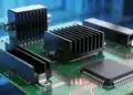
Device embedding in PCBs is a transformative technology that enhances miniaturization, functional reliability, and thermal management. The process strategically integrates components within PCB layers, optimizing space and improving performance.

Key Benefits of Device Embedding

  1. Miniaturization: Embedding components reduces board real estate requirements, enabling compact device designs without compromising functionality.
    • Custom Packaging: Create bespoke packages for specific circuitry needs.
    • Space Efficiency: Utilize internal PCB layers to add components beyond the surface.
  2. Performance & Functionality:
    • Integrated Shielding: Embedded components benefit from natural EMI shielding using surrounding copper layers.
    • Short Signal Paths: Reduced signal travel distances improve speed and reduce power loss.
    • Anti-Plagiarism Measures: Concealing components within layers protects against reverse engineering.
  3. Reliability:
    • Environmental Protection: Embedded components are less susceptible to moisture, mechanical stress, and temperature extremes.
    • Enhanced Thermal Management: Better heat dissipation through direct copper contact.

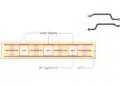
Technical Process of Device Embedding

  1. Inner Layer Preparation:
    • Structuring copper layouts.
    • Applying solder resist to create solder windows for component placement.
    • Surface finishing with modified chemical tin to aid soldering and adhesion.
  2. Component Assembly:
    • Standard SMD processes for component placement.
    • Rigorous cleaning protocols to ensure void-free lamination.
  3. Multilayer Stack-Up and Lamination:
    • Use of prepregs with precision cutouts forming virtual cavities.
    • High-pressure, vacuum-assisted lamination to encapsulate components seamlessly.
  4. Finishing Processes:
    • Drilling, plating, and final outer layer structuring.
    • Comprehensive testing tailored to project specifications (ICT, functional tests).

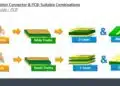
Case Study: PCB Sample “We Embed”

The sample features:

  • Six Copper Layers with components embedded on layer 4.
  • Component Variety: LEDs, resistors, capacitors, and active ICs in diverse packages (UDFN, TSSOP, QFN).
  • Functional Demonstration: A running light circuit accessible via USB power.

Design Considerations and Testing

  • Layer Count Flexibility: From minimal configurations to complex multi-layered designs.
  • Component Thickness: Custom stack-ups accommodating various component heights.
  • Testing Protocols: Defined collaboratively with clients to meet application-specific reliability standards.

Cost Implications

Costs are influenced by:

  • Base PCB technology (rigid, flex, HDI).
  • BOM specifics and component sourcing.
  • Assembly complexity and testing requirements.

Conclusion

Device embedding significantly advances PCB design by enabling compact, high-performance, and reliable electronic solutions. For more information, technical guidelines, and sample requests, visit WE Electronic’s website or reach out to their technical support team.

Related

Source: Würth Elektronik

Recent Posts

Heatsink Design and Thermal Interface Materials for Reliable Electronics

27.4.2026
142

Würth Elektronik Introduces Lead-Free SMT Spacers

11.2.2026
93

Coaxial Connectors and How to Connect with PCB

17.12.2025
887

PCB Manufacturing, Test Methods, Quality and Reliability

18.6.2026
356

Murata Releases World’s First Inner Cavity-Structure Ultra-Low-Loss LCP Flexible Substrate

10.12.2025
146

Connector PCB Design Challenges

3.10.2025
98

Panasonic Industry to Double Production of MEGTRON PCB Materials

15.9.2025
111

Glass Core Technology Breakthrough Potential for High-Speed Interconnects

5.1.2026
302

What Track Width To Use When Routing PCB

6.6.2025
183

Upcoming Events

Jun 30
17:00 - 18:00 CEST

PSMA Capacitor Committee Webinar: High Voltage Pulse Capacitors

Jul 14
16:00 - 17:00 CEST

EMC Design Essentials: Mastering Varistors and Common Mode Chokes

Jul 21
16:00 - 17:00 CEST

Safety by design: X and Y Interference suppression capacitors for power line filters

View Calendar

Popular Posts

  • Boost Converter Design and Calculation

    0 shares
    Share 0 Tweet 0
  • Buck Converter Design and Calculation

    0 shares
    Share 0 Tweet 0
  • LLC Resonant Converter Design and Calculation

    0 shares
    Share 0 Tweet 0
  • Flyback Converter Design and Calculation

    0 shares
    Share 0 Tweet 0
  • MLCC and Ceramic Capacitors

    0 shares
    Share 0 Tweet 0
  • Nvidia Vera Rubin: Why One AI Rack Needs So Many More MLCC Capacitors

    0 shares
    Share 0 Tweet 0
  • Earthing Systems and IEC Classification Explained

    0 shares
    Share 0 Tweet 0
  • SEPIC Converter Design and Calculation

    0 shares
    Share 0 Tweet 0
  • Dual Active Bridge (DAB) Topology

    0 shares
    Share 0 Tweet 0
  • MLCC Case Sizes Standards Explained

    0 shares
    Share 0 Tweet 0

Newsletter Subscription


Passive Components Blog

© EPCI - Leading Passive Components Educational and Information Site

  • Home
  • Privacy Policy
  • EPCI Membership & Advertisement
  • About

No Result
View All Result
  • Home
  • Knowledge Blog
  • Dossiers
  • PCNS

© EPCI - Leading Passive Components Educational and Information Site

This website uses cookies. By continuing to use this website you are giving consent to cookies being used. Visit our Privacy and Cookie Policy.
Go to mobile version