


This video and article delve into the groundbreaking potential of Glass Core Technology (GCT), as discussed in Judy Warner’s episode of The EEcosystem Podcast with Steve Hillerich, Product Manager at Samtec. GCT is poised to revolutionize high-speed interconnects, miniaturization, and system integration by meticulously controlling every aspect of glass substrate development, spanning from TGV drilling to RDL patterning.
Introduction
Glass Core Technology (GCT) is a glass‑based interconnect platform that uses metallized through‑glass vias (TGVs) and fine‑pitch redistribution layers (RDLs) to route high‑frequency and high‑speed signals very close to the silicon die. It targets environments where conventional organic substrates or ceramics reach limits in frequency, density, or mechanical performance.
The core technical problem addressed is how to achieve low‑loss, high‑density, and mechanically stable interconnects at millimeter‑wave and sub‑THz frequencies, while supporting advanced multi‑chip and 3D packaging.
Key points
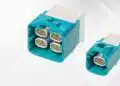
- Glass Core Technology uses a glass wafer or panel with drilled vias that are fully metallized to form TGVs, combined with thin‑film RDL on one or both sides.
- The same glass structure can be used as a substrate with die mounted directly on it, or as an interposer between active devices and other substrates in 2.5D/3D assemblies.
- TGVs are formed by laser and/or chemical drilling, then seeded and plated to create straight‑wall, fully filled, planar vias suitable for RF and high‑speed use.
- RDL patterns are created with semiconductor‑style lithography and thin‑film processes, enabling fine line/space and dense fan‑out from die bumps or pillars.
- Glass materials can be selected (borosilicate, fused silica, synthetic quartz, sapphire, etc.) to tune dielectric properties and coefficient of thermal expansion (CTE).
- Low‑loss glass supports operation above 300 GHz, with close agreement between electromagnetic simulations and measured performance.
- Hermetic TGVs are achievable, which is relevant for harsh environments, vacuum or pressure‑sensitive systems, and some biomedical or MEMS applications.
- RF passives such as filters, dividers, capacitors, and waveguides can be implemented directly in the glass using TGV and RDL structures.
- Process integration covers drilling, via metallization, RDL formation, and assembly in a cleanroom environment using modified semiconductor tools.
- A Process Design Kit (PDK) is being developed to provide parameterized building blocks and design rules for GCT in standard EDA workflows.
Background and motivation
At high data rates and RF/millimeter‑wave frequencies, interconnect structures become a dominant constraint on system performance. Traditional organic laminates and many ceramic technologies have limitations in achievable feature size, dielectric loss, dimensional stability, and integration of multiple dies and RF structures.
The industry trend toward multi‑chip modules, 2.5D interposers, and 3D stacking creates demand for substrates that can support short, precisely controlled signal paths, fine‑pitch connections, and reliable operation across wide temperature ranges. Glass offers a tunable material family with favorable dielectric properties, good thickness uniformity, and potential for CTE matching to both semiconductor and surrounding structures.
Glass Core Technology structure and function
In GCT, the starting point is a glass wafer or panel that will become the “core.” This core is processed to include:
- Through‑glass vias: holes drilled through the glass and metallized to create vertical conductors.
- Redistribution layers: patterned metal layers on one or both sides for signal routing, power, and ground.
Depending on the assembly, this glass core can:
- Serve as a substrate, with active die attached via bumps, copper pillars, or other interconnects.
- Act as an interposer, placed between active silicon and an organic or ceramic carrier to provide dense fan‑out and RF structures.
The structure is compatible with 2.5D and 3D integration, where multiple dies are arranged side by side or stacked, with connections routed through and across the glass core.
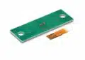
TGV formation and metallization
TGVs are central to the technology. Their formation involves:
- Drilling: Vias are created using laser drilling, chemical etching, or a combination, tuned to produce consistent via geometry through the glass thickness.
- Seed layer: A conductive seed layer is deposited, often by sputtering, to coat the via walls and surfaces.
- Plating: Electroplating fills the vias, typically with copper, to form continuous solid or near‑solid conductors.
The process aims for straight‑wall, fully filled vias that terminate flush with the glass surface after planarization. This avoids hourglass shapes and internal voids that can trap gases or liquids and lead to reliability issues under thermal cycling or vacuum processing.
Hermeticity of the vias can be verified by helium leak testing, which is relevant for applications requiring sealed cavities or resistance to environmental ingress.
Redistribution layers and fine‑pitch routing
On each side of the glass core, thin‑film RDLs are formed using lithography and metal deposition techniques related to semiconductor back‑end processing. Typical steps include:
- Dielectric coating or surface preparation of the glass.
- Metal seed deposition.
- Photoresist patterning for line/space and pads.
- Electroplating of copper traces and pads.
- Resist stripping and etching of unwanted metal.
This approach supports fine‑pitch traces and small pads compatible with advanced die bump pitches and high‑density fan‑out. Because the glass is flat and thickness‑controlled, RDL layers can be accurately aligned, and multi‑layer routing with interlayer vias is possible.
Material selection and electrical behavior
“Glass” encompasses multiple compositions, and the choice impacts both electrical and mechanical behavior. Common options mentioned include:
- Borosilicate glass.
- Fused silica.
- Synthetic quartz.
- Sapphire.
Key parameters are dielectric constant, loss tangent, and CTE over the operating temperature range. Low‑loss materials such as fused silica or synthetic quartz support applications beyond 300 GHz, where line and via losses must be tightly controlled.
Designers can simulate structures using these material properties and obtain results that align closely with measured behavior, which simplifies tuning of RF structures and reduces iteration cycles.
Mechanical and packaging aspects
Glass wafers offer:
- Tight thickness tolerance and flatness.
- Smooth surfaces suitable for fine‑pitch bonding.
- Potential to match CTE to silicon and other materials through composition selection.
These properties are advantageous for:
- 2.5D assemblies with multiple dies on one glass core.
- 3D stacks using copper pillars, thermo‑compression bonding, or anodic bonding.
Mechanical reliability depends on managing stresses between glass, metal, and attached components during temperature cycling; via geometry and fill quality are critical factors in avoiding cracking or delamination.
Embedded RF passives and structures
Beyond simple routing, TGV and RDL patterns can implement RF passives directly in the glass. Examples include:
- Transmission‑line‑based bandpass or bandstop filters.
- Dividers and combiners using distributed or lumped concepts.
- Capacitors formed by overlapping metal plates separated by glass or dielectric layers.
- Waveguides or quasi‑waveguide structures defined by metal boundaries and vias.
Embedding these functions reduces the number of discrete components and interconnect transitions, which is beneficial at high frequency where each interface contributes loss and potential reflections.
Process integration and tooling
The process flow for GCT uses semiconductor‑class tools but adapted for glass processing. This includes:
- Cleanroom environments to control contamination.
- Lithography equipment for fine‑pitch RDL patterning.
- Sputter and plating tools for seed and via fill metals.
- Laser systems or etchers configured for transparent substrates.
Key process aspects—such as via drilling conditions, plating chemistry, and thermal treatments—are tuned to maintain via integrity and adhesion between metals and glass. Running drilling, metallization, RDL, and assembly in a single integrated flow allows tight control over variations and supports consistent electrical and mechanical performance.
Design enablement and PDK concept
Because each glass core design is effectively custom and uses materials outside typical PCB libraries, a Process Design Kit is being developed to integrate GCT into standard RF and packaging design tools. The intended contents include:
- Parameterized elements (e.g., filters, waveguide segments, capacitors) implemented in glass.
- Process‑specific design rules for via sizes, line widths, spacing, and stack‑ups.
- Verified models correlating layout, simulation, and measured performance for key building blocks.
This is intended to let designers work with higher‑level functional blocks instead of manually designing each RF structure from raw material data and process constraints.
Conclusion
Glass Core Technology provides a glass‑based interconnect platform with metallized TGVs and lithographically defined RDLs aimed at high‑frequency and high‑density electronic systems. Its key technical attributes are controllable dielectric behavior, fine‑pitch routing, hermetic vias, and compatibility with advanced 2.5D and 3D packaging flows.
By selecting appropriate glass compositions and process parameters, designers can implement short, low‑loss interconnects and embedded RF passives that behave predictably from simulation through fabrication. As process design kits mature, GCT is positioned to become another substrate option alongside organic laminates and ceramics for engineers addressing RF, millimeter‑wave, sub‑THz, MEMS, and specialized high‑speed applications.youtube
References
- Why Glass Core is the Next Leap in High-Speed Design, Engineering EEcosystem Podcast (YouTube). https://www.youtube.com/watch?v=LvslK76XOKY
- Samtec – Glass Core Technology (GCT). https://www.samtec.com/GCT
FAQ about Glass Core Technology
Glass Core Technology (GCT) is a glass-based interconnect platform that uses metallized through-glass vias (TGVs) and thin-film redistribution layers (RDLs) to route high-frequency and high-speed signals very close to the silicon die. It can function as a substrate or an interposer in 2.5D and 3D packaging.
TGVs are created by laser and/or chemical drilling through the glass, followed by deposition of a conductive seed layer and electroplating with copper. The process targets straight-wall, fully filled vias that are planar with the glass surface to ensure low loss and high reliability under thermal and mechanical stress.
Glass enables much finer features than typical PCBs, offers excellent thickness uniformity and flatness, and can be composition-tailored for coefficient of thermal expansion (CTE) matching. Certain glass types, such as fused silica and synthetic quartz, also provide low dielectric constant and loss tangent, supporting operation well beyond 300 GHz.
GCT provides low-loss interconnects at RF, millimeter-wave, and sub-THz frequencies, with short, compact routing paths and hermetic TGVs. Designers report strong correlation between electromagnetic simulations and measured results, which reduces design iterations and improves predictability of RF structures implemented in glass.
Yes. By shaping TGV arrays and RDL patterns, designers can embed RF passives such as filters, dividers, crossovers, capacitors, and waveguide-like structures directly in the glass. This reduces discrete component count, interconnect transitions, and overall insertion loss in high-frequency modules.
GCT is suited to RF and telecom infrastructure beyond 6G, high-frequency datacom links, biomedical and implantable devices, MEMS and sensor systems requiring hermeticity, advanced handheld or analytical instruments, and selected defense applications where conventional PCB or ceramic substrates hit limits in size, frequency, or robustness.
The high planarity and controlled thickness of glass support fine-pitch bonding using copper pillars, thermo-compression, or anodic bonding. Multiple dies can be placed side by side or stacked on a single glass core, with dense RDL routing and vertical connections implemented through TGVs.
Reliability depends on via geometry, full via fill, and adhesion between metals and glass. Straight-wall, fully filled TGVs avoid voids that can trap gas or liquids, which helps prevent failures under thermal cycling and vacuum processing. Hermetic vias are validated using helium leak testing for sensitive applications.
Running drilling, via metallization, RDL formation, and assembly within a single integrated process flow enables tighter control over variations and stress conditions. This improves consistency in electrical behavior and mechanical robustness, compared to distributed flows where different vendors handle separate steps.