Passive Components Blog
No Result
View All Result
  • Home
  • NewsFilter
    • All
    • Aerospace & Defence
    • Antenna
    • Applications
    • Automotive
    • Capacitors
    • Circuit Protection Devices
    • electro-mechanical news
    • Filters
    • Fuses
    • Inductors
    • Industrial
    • Integrated Passives
    • inter-connect news
    • Market & Supply Chain
    • Market Insights
    • Medical
    • Modelling and Simulation
    • New Materials & Supply
    • New Technologies
    • Non-linear Passives
    • Oscillators
    • Passive Sensors News
    • Resistors
    • RF & Microwave
    • Telecommunication
    • Weekly Digest

    Binder Hybrid Connector Simplifies One Cable Automation

    Tapped Inductor Buck Converter Fundamentals

    TAIYO YUDEN Releases Mini Metal Power Inductors

    Molecular Memristor Shows Record 145 kH Emergent Inductance

    Planar vs Conventional Transformer: When it Make Sense

    Researchers Propose Next‑Gen Compact Memory Using Ultra-thin Ferroelectric Capacitors

    Nichicon ADN Automotive Hybrid Aluminum Capacitors Now Available in EMEA

    Wk 19 Electronics Supply Chain Digest

    Electrocaloric Multilayer Capacitors: Towards Quiet, Solid‑State Cooling Around Room Temperature

    Trending Tags

    • Ripple Current
    • RF
    • Leakage Current
    • Tantalum vs Ceramic
    • Snubber
    • Low ESR
    • Feedthrough
    • Derating
    • Dielectric Constant
    • New Products
    • Market Reports
  • VideoFilter
    • All
    • Antenna videos
    • Capacitor videos
    • Circuit Protection Video
    • Filter videos
    • Fuse videos
    • Inductor videos
    • Inter-Connect Video
    • Non-linear passives videos
    • Oscillator videos
    • Passive sensors videos
    • Resistor videos

    Tapped Inductor Buck Converter Fundamentals

    Planar vs Conventional Transformer: When it Make Sense

    Modeling Fringing Field Losses in Inductors & Transformers

    Why Power Inductors Use a Ferrite Core With an Air Gap

    Transformer-Based Power-Line Harvester Magnetic Design

    Thermal Modeling of Magnetics

    Standard vs Planar LLC transformers Comparison for Battery Chargers

    How Modern Tools Model Magnetic Components for Power Electronics

    Advanced Loss Modeling for Planar Magnetics in the Frenetic Planar Tool

    Trending Tags

    • Capacitors explained
    • Inductors explained
    • Resistors explained
    • Filters explained
    • Application Video Guidelines
    • EMC
    • New Products
    • Ripple Current
    • Simulation
    • Tantalum vs Ceramic
  • Knowledge Blog
  • DossiersNew
  • Suppliers
    • Who is Who
  • PCNS
    • PCNS 2025
    • PCNS 2023
    • PCNS 2021
    • PCNS 2019
    • PCNS 2017
  • Events
No Result
View All Result
Passive Components Blog
No Result
View All Result

PCBs Mini, Micro and Microvia; Würth Elektronik Webinar

11.8.2025
Reading Time: 4 mins read
A A

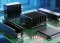
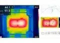
Partial vias play a decisive role in the miniaturization of printed circuit boards. Learn more insights in this Würth Elektronik Webinar.

These are buried vias and microvias, which can be combined in different ways. We call microvias placed directly in solder pads “microvia-in-pad”. This saves valuable space, and since microvias are very small blind holes, they can also be integrated into very small solder pads. This is crucial for unbundling miniaturized or complex components such as micro BGAs.

RelatedPosts

Würth Elektronik Introduces Compact Flat-wire SMT Power Inductors for Automotive

Heatsink Design and Thermal Interface Materials for Reliable Electronics

Würth Elektronik Expanded Capacity for Validation and Services in Asia

In this webinar, learn more about

  • our sample WE.microbga and what you can learn from it
  • the current design rules of the MICROVIA.hdi technology and their application
  • the routing of a BGA component with pitch 0.4 mm
  • the advantages of MICROVIA.hdi technology in terms of signal integrity
  • impedance calculations

Advances in HDI PCB Design: A Technical Overview

Introduction

High-Density Interconnect (HDI) technology is revolutionizing the electronic circuit board industry with its ability to support complex designs and high-speed data transmission. This article explores the intricacies of HDI Printed Circuit Boards (PCBs), focusing on the Microvia technology and its applications, as presented in a recent webinar hosted by Andrea Schil and featured expert Andreas Drea from V Electronic Circuit Board Technology.

Understanding HDI PCB Sample

The HDI PCB sample represents a typical industrial board used in automotive, sensor applications, and various machinery. It integrates power lines, memory chips, QFP components, and BGA units. A closer look reveals details hidden beneath the surface, such as specific impedance requirements, runtime matching, and complex stackups.

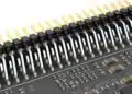
BGA Components and Routing Techniques

  • Standard BGA (0.8 mm pitch): Utilizes through-hole drilling for routing, requiring multiple layers (typically 8-10) to accommodate all connections.
  • Microvia BGA (0.4 mm pitch): Employs laser-drilled vias, significantly reducing the number of layers needed and saving space, thus lowering production costs.

Stackup Configurations

Key features include:

  • Buried Vias: Resin-filled for enhanced reliability.
  • Staggered & Stacked Microvias: Optimized for different performance requirements.
  • Galvanic Processes: Sequential layer additions with meticulous copper plating techniques ensure structural integrity.

Production Insights

Inner Layer Manufacturing

Starting with a copper-clad laminate:

  • Photolithography: Defines circuit patterns.
  • Etching: Removes excess copper, creating precise trace geometries.

Via Formation and Filling

  • Laser Drilling: Achieves high precision for microvias without significant wear.
  • Filling Processes: Utilize copper or resin to enhance conductivity and mechanical strength.

Cost Considerations

  • Laser Drilling vs. Mechanical Drilling: While laser drilling has higher setup costs, it offers lower variable costs per via, making it cost-effective for high-density designs.

Impedance Control

Impedance is influenced by:

  • Line Width and Layer Spacing: Primary factors in determining signal integrity.
  • Material Properties: Dielectric constants play a secondary role.

V Electronic offers three levels of impedance services:

  1. Calculation: During the design phase.
  2. Manufacturing Control: Ensuring consistency across production.
  3. On-Panel Testing: Verifying impedance for each production batch.

Design Recommendations

  • Utilize Microvias Extensively: Not just in BGA areas but across the board for cost efficiency.
  • Optimize Line and Space Parameters: To enhance production yield and reduce costs.
  • Early Collaboration: Engage with PCB manufacturers early to mitigate redesign efforts and ensure manufacturability.

Conclusion

Advancements in HDI technology, particularly Microvia and impedance control techniques, offer significant benefits in efficiency, performance, and cost. Early-stage collaboration with PCB manufacturers like V Electronic is crucial for optimizing these advantages in electronic circuit board designs.

Related

Source: Würth Elektronik

Recent Posts

Heatsink Design and Thermal Interface Materials for Reliable Electronics

27.4.2026
35

Coaxial Connectors and How to Connect with PCB

17.12.2025
589

PCB Manufacturing, Test Methods, Quality and Reliability

17.12.2025
281

Connector PCB Design Challenges

3.10.2025
80

What Track Width To Use When Routing PCB

6.6.2025
160

IPC Class 2 vs Class 3 Solder Joints Requirements Explained

27.2.2025
1.3k

How to Determine Chip Temperature

3.1.2025
405

Die and Wire PCB Bonding Explained

1.7.2025
394

EMI Shielding Challenges

1.7.2025
36

Upcoming Events

May 19
16:00 - 17:00 CEST

Designing Qi2 Wireless Power Systems: Practical Development and EMC Optimization

Jun 2
16:00 - 17:00 CEST

Calculation, Simulation and Measurement of 800V EMC Filters

Jun 16
16:00 - 17:00 CEST

EMC with EMC – EMC‑compliant design with electromechanical connectors

View Calendar

Popular Posts

  • Buck Converter Design and Calculation

    0 shares
    Share 0 Tweet 0
  • Boost Converter Design and Calculation

    0 shares
    Share 0 Tweet 0
  • Flyback Converter Design and Calculation

    0 shares
    Share 0 Tweet 0
  • LLC Resonant Converter Design and Calculation

    0 shares
    Share 0 Tweet 0
  • MLCC and Ceramic Capacitors

    0 shares
    Share 0 Tweet 0
  • Dual Active Bridge (DAB) Topology

    0 shares
    Share 0 Tweet 0
  • Capacitor Charging and Discharging

    0 shares
    Share 0 Tweet 0
  • What Electronics Engineer Needs to Know About Passive Low Pass Filters

    0 shares
    Share 0 Tweet 0
  • Ripple Current and its Effects on the Performance of Capacitors

    3 shares
    Share 3 Tweet 0
  • MLCC Case Sizes Standards Explained

    0 shares
    Share 0 Tweet 0

Newsletter Subscription


Passive Components Blog

© EPCI - Leading Passive Components Educational and Information Site

  • Home
  • Privacy Policy
  • EPCI Membership & Advertisement
  • About

No Result
View All Result
  • Home
  • Knowledge Blog
  • PCNS

© EPCI - Leading Passive Components Educational and Information Site

This website uses cookies. By continuing to use this website you are giving consent to cookies being used. Visit our Privacy and Cookie Policy.
Go to mobile version