


Nanomechanical systems developed at TU Wien have achieved unprecedented precision and miniaturization, paving the way for their integration into ultra-high-resolution atomic force microscopes in the future. The groundbreaking findings about their research High Aspect Ratio, Superconducting Vacuum Gap Capacitor NEMS with Plate Distances Down to 32 nm have been published in the journal Advanced Materials Technologies.
Introduction
The article presents the design, fabrication, and low‑temperature characterization of high‑aspect‑ratio, superconducting vacuum gap capacitor nano‑electromechanical systems (NEMS) with capacitor plate separations down to 32 nm. These devices are based on aluminium membranes suspended above a fixed aluminium bottom electrode on a silicon substrate, forming a vacuum capacitor integrated into an LC resonator. The work targets large electromechanical coupling for quantum and sensing applications, while maintaining high wafer‑level yield.
Vacuum gap capacitor NEMS are a key building block for quantum electromechanics, enabling strong coupling between a mechanical membrane mode and a microwave electrical cavity. However, their fabrication is technologically demanding due to nanometer‑scale gaps, thin suspended films, and stringent stress control requirements. The study addresses these challenges by combining stress‑engineered sputter deposition, controlled oxidation, and optimized sacrificial layer etching to realize robust devices on CMOS‑compatible silicon wafers instead of sapphire.
The authors further demonstrate an integrated aluminium nitride (AlN) piezoelectric actuator for coherent mechanical drive and verify electromechanical coupling at cryogenic temperatures around 400 mK. This combination of fabrication methodology, stress optimization strategy, and low‑temperature validation provides a process blueprint for high‑yield, strongly coupled nano‑electromechanical capacitors suitable for quantum and sensing applications.
Key points
- Realization of aluminium vacuum gap capacitor NEMS with fixed bottom electrode and free‑standing top membrane, achieving plate gaps down to 32 nm at cryogenic temperatures.
- Fabrication on silicon wafers with oxi‑nitride coatings, improving CMOS compatibility and cost compared to sapphire substrates, at the expense of lower electrical cavity Q due to higher dielectric loss.
- Introduction of a thin silicon capping layer on the top aluminium electrode to enforce simultaneous oxidation on both sides, preventing stress‑induced membrane collapse after sacrificial release.
- Systematic stress engineering of sputtered aluminium via power/pressure optimization and a binary‑search‑based calibration to minimize vertical stress gradients in 80–120 nm top films.
- Use of an empirical stress–thickness model to fit average stress σ(t) and extract a parameter β that quantifies how fast stress approaches a plateau, guiding the choice of sputter power.
- Demonstration of wafer‑level yields above 90% for membranes with radii comparable to literature values, and around 50% even for significantly larger radii.
- Finite‑element simulations of thermal contraction from 300 K to near 0 K showing about 120 nm reduction of the gap for typical geometries, used to back‑design room‑temperature gaps that remain non‑collapsed at mK temperatures.
- Room‑temperature laser Doppler vibrometry (LDV) characterization showing a first mechanical eigenmode around 2.03 MHz with Q ≈ 500, and multiple higher‑order modes driven by the integrated AlN piezo actuator.
- Cryogenic RF transmission measurements at 400 mK revealing an electrical resonance around 1.29 GHz and allowing extraction of a capacitor gap of 32 nm, with power‑dependent nonlinear behavior attributed to kinetic inductance of the thin‑film spiral inductor.
- Identification of multiple electrical modes and discussion of trade‑offs between high electromechanical coupling (small gaps, larger radii) and fabrication yield and stability against membrane collapse.
Extended summary
Vacuum gap capacitor NEMS rely on the strong dependence of an LC cavity’s resonance frequency on the separation between a fixed plate and a movable membrane forming a nanometer‑scale capacitor. The mechanical motion of the membrane modulates the electrical cavity frequency, enabling energy exchange between mechanical and electrical modes. A central figure of merit is the parametric coupling rate , which quantifies how strongly cavity frequency responds to membrane displacement. The devices studied here aim at large G through small capacitor gaps, minimized parasitic capacitance, and adequately high cavity frequency, while also ensuring practical wafer‑scale yields.
The parametric coupling is defined via the derivative of the cavity resonance frequency with respect to mechanical displacement , where the vacuum gap capacitance and the parasitic capacitance form the effective capacitance. The article introduces conceptually as the change in caused by a displacement‑induced change in gap . The authors emphasize that reducing the static gap and minimizing relative to drastically enhances , because a smaller gap increases the capacitance sensitivity to displacement and, consequently, the device responsivity. Increasing the number of photons in the electrical cavity can further enhance the effective coupling, but is limited by nonlinearities and local heating that can suppress superconductivity, so fabrication‑level improvements to are particularly attractive.
The fabrication starts from a 4‑inch silicon wafer covered with a stress‑compensated oxi‑nitride stack (about 250 nm SiO plus 70 nm SiN). The bottom electrode is a 30 nm aluminium layer deposited by DC magnetron sputtering and patterned to form the fixed capacitor pad and interconnects. A sacrificial silicon layer, typically 300 nm thick, is then sputter‑deposited to fully cover the bottom pad and part of the future inductor line, defining the nominal vacuum gap. On top of that, a 300 nm AlN piezoelectric film is locally deposited near the future membrane to enable integrated mechanical actuation. Finally, a top aluminium layer of roughly 100 nm is sputtered and patterned to form the movable membrane, the spiral inductor, the RF transmission line, and a second piezo contact pad.
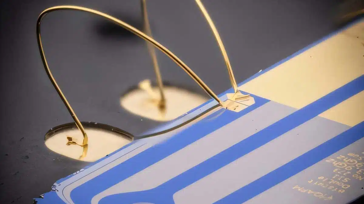
After front‑side structuring, a Bosch deep reactive ion etch from the backside defines chip outlines, followed by spray‑coated photoresist on the backside to protect exposed silicon. The sacrificial silicon layer is removed by XeF dry etching, which undercuts the membrane to create the vacuum gap between top and bottom electrodes. Optical images show chips wire‑bonded to PCBs with coplanar waveguides for RF access and side contacts for the piezoelectric actuator, while SEM images highlight the compact integration of the spiral inductor, membrane capacitor, and piezo region.
A key fabrication challenge is preventing membrane collapse during or after sacrificial etching. Initially, the underside of the top aluminium layer is protected from air during processing, while the top surface oxidizes to about 10 nm AlO almost immediately after exposure. This asymmetric oxidation shifts the neutral axis and induces compressive stress gradients, which can drive the membrane either to buckle upward (increasing the effective gap) or to buckle downward and contact the bottom electrode (shorting the capacitor). To address this, the authors insert a thin (~10 nm) sputtered silicon capping layer immediately after depositing the top aluminium, without breaking vacuum. This layer prevents premature oxidation of the top surface. During XeF etching there is no oxygen, so oxidation is suppressed on both sides. Only when the sample is removed from the etcher and exposed to air do both sides oxidize simultaneously, forming symmetric oxide layers and eliminating the oxidation‑induced stress asymmetry. This simple modification is crucial for obtaining stable, non‑collapsed membranes.
Beyond oxidation symmetry, the vertical normal stress gradient within the aluminium layer must be controlled. Sputtered thin films naturally exhibit stress variations across thickness due to process conditions, leading to upward buckling for positive gradients or downward buckling for negative gradients. The authors adopt an empirical model for the average normal stress as a function of film thickness :
where is the steady‑state stress, and , describe how stress approaches its plateau with increasing thickness. A larger indicates faster convergence to the steady‑state value and thus a smaller stress gradient within the thickness range of interest (here approximately 80–120 nm for the top electrode). The goal is to identify deposition conditions that maximize and ensure that the stress is effectively constant across the membrane thickness, minimizing curvature and buckling.
The stress is measured using a wafer‑bow technique on test wafers that replicate the Al/Si stack (30 nm Al bottom, 300 nm Si sacrificial layer), followed by varying top aluminium thicknesses. Initial recipes using 300 W sputter power and 3 µbar argon pressure show that average stress increases with thickness and only plateaus beyond ~300 nm, which is not ideal for 100 nm membranes. Raising the power to 600 W exacerbates this, as plasma‑induced heating of the silicon substrate, combined with the large thermal expansion mismatch between aluminium and silicon, leads to higher stress and slower convergence. Lower powers of 100 W and 50 W at 3 µbar are subsequently explored, yielding earlier stress saturation and visually smooth, reflective films even at larger thicknesses. Fitting the empirical model reveals that lower power increases , confirming that reducing plasma heating improves stress uniformity.
To efficiently find the optimum power for minimal stress gradient, the authors adopt a binary search strategy at fixed pressure (3 µbar). For each candidate power between 100 W and 250 W, two wafers are deposited with aluminium thicknesses of 100 nm and 1000 nm, respectively, and their average stresses are measured. The optimum power is where these two stresses intersect, indicating that the stress has already plateaued at 100 nm and is similar to that at 1000 nm, implying a small gradient over the thickness of interest. This procedure is repeated with the system in different states, leading to optima around 105–110 W in one case and 50 W in another, with the latter showing a particularly large (~6.01 × 10⁻² n−1m). The final device recipe uses 50 W, 3 µbar, with stress measurements confirming a plateau between about 40 nm and 60 nm thickness. This method significantly reduces calibration time and is robust against changes in the sputtering environment.
Using the optimized recipe and oxidation control, the authors fabricate three wafers, each with about 400 vacuum gap capacitors. Visual inspection and random LDV verification suggest room‑temperature yields above 90% for membrane radii similar to those reported in literature, and still around 50% for much larger radii. However, these yields must be preserved at cryogenic temperatures where the devices operate in the superconducting regime. Thermal contraction is critical: aluminium has a linear expansion coefficient of roughly 2.3 × 10 K while silicon is about 3.3 × 10 K, so cooling toward absolute zero causes the aluminium membrane to contract more than the substrate, effectively pulling it closer to the bottom electrode. To predict the low‑temperature gap and avoid collapse, finite‑element simulations in COMSOL are performed for a representative aluminium membrane (radius and initial gap of 300 nm). Cooling from 300 K to 0 K produces a calculated gap reduction of about 120 nm. These results are used to back‑calculate suitable room‑temperature gaps and sacrificial thicknesses for different membrane radii and slopes, balancing electromechanical coupling against the risk of low‑temperature collapse.
Mechanical characterization at room temperature uses a Polytec MSA‑500 LDV setup. Thermal motion of a membrane (with radius aligned to typical literature designs) reveals a first eigenmode at about 2.027 MHz with a quality factor around 500 in vacuum, confirming that the membrane is released and free to move. With a 1 V drive applied to the integrated AlN piezo actuator, larger amplitude oscillations and higher mechanical modes are observed. Several eigenmodes are identified and matched to finite‑element mode shapes. These measurements validate that the process yields functional, high‑Q micromechanical resonators with integrated actuation.
Electromechanical coupling is demonstrated at cryogenic temperatures using a He evaporation cryostat reaching roughly 400 mK, well below the aluminium critical temperature (~1.3 K). The measurement chain includes a 1–2.5 GHz band‑pass filter, a 30 dB attenuator at room temperature, a coplanar waveguide coupled inductively to the on‑chip spiral inductor, and a cryogenic amplifier on the output. Vector network analyzer (VNA) transmission measurements show a clear resonance at approximately 1.29 GHz. By matching the measured response with a lumped‑element model in Cadence AWR, the authors infer a capacitor plate gap of 32 nm at low temperature. This confirms that the combination of sacrificial gap design, thermal‑contraction modeling, and stress engineering can reliably produce extremely small, yet non‑collapsing, vacuum gaps.
By varying input power, two additional electrical modes with narrower linewidths are detected, indicating multiple resonant pathways in the coupled LC network. At higher powers, the fundamental electrical mode exhibits a downward frequency shift and reduced quality factor, behavior consistent with nonlinear inductance arising from kinetic inductance in the thin‑film aluminium spiral. These observations are important for future designs, as they highlight trade‑offs between strong drive for enhanced coupling and the onset of nonlinearities and heating that may limit performance.
Overall, the work provides a complete, experimentally validated route to high‑aspect‑ratio, superconducting vacuum gap capacitor NEMS on silicon. It combines analytical modeling of stress and coupling, empirical optimization of sputter conditions, finite‑element simulations of thermal contraction, and detailed mechanical and RF characterization. The devices achieve sub‑50‑nm vacuum gaps at mK temperatures, high mechanical Q at MHz frequencies, and GHz electrical resonances suitable for quantum and high‑sensitivity sensing schemes.
Conclusion
The article demonstrates a robust, stress‑engineered fabrication process for superconducting vacuum gap capacitor NEMS with plate separations as small as 32 nm and wafer‑scale yields suitable for research‑level sensing and quantum electromechanics. Key innovations include symmetric oxidation of aluminium membranes via an in‑vacuum silicon cap, systematic optimization of sputtered aluminium stress using a binary search on deposition power, and FEM‑guided design of room‑temperature gaps that remain safe at cryogenic temperatures. Integrated AlN piezoactuation and GHz microwave readout confirm both mechanical and electrical performance at room temperature and 400 mK.
Limitations arise from the use of silicon substrates, which increase dielectric loss and lower electrical cavity Q compared to sapphire, making sideband‑resolved quantum operations more challenging. In addition, the grain structure of aluminium, and its impact on mechanical and electrical quality factors, has not yet been fully optimized and calls for further studies that disentangle different loss mechanisms. Future work may explore alternative substrate stacks, refined metallization to enhance Q, systematic investigation of grain‑size effects, and demonstration of concrete sensing or quantum protocols such as bifurcation‑based sensing, parametric amplification, or multi‑mode quantum state control using the presented NEMS platform.
References
- D. Ignat, et al., “High Aspect Ratio, Superconducting Vacuum Gap Capacitor NEMS with Plate Distances Down to 32 nm,” Advanced Materials Technologies, 2025, Wiley Online Library, https://doi.org/10.1002/admt.202401909