Passive Components Blog
No Result
View All Result
  • Home
  • NewsFilter
    • All
    • Aerospace & Defence
    • Antenna
    • Applications
    • Automotive
    • Capacitors
    • Circuit Protection Devices
    • electro-mechanical news
    • Filters
    • Fuses
    • Inductors
    • Industrial
    • Integrated Passives
    • inter-connect news
    • Market & Supply Chain
    • Market Insights
    • Medical
    • Modelling and Simulation
    • New Materials & Supply
    • New Technologies
    • Non-linear Passives
    • Oscillators
    • Passive Sensors News
    • Resistors
    • RF & Microwave
    • Telecommunication
    • Weekly Digest

    RF Inductors: Selection and Design Challenges for High-Frequency Circuits

    Wk 45 Electronics Supply Chain Digest

    Transformer Safety IEC 61558 Standard

    ESR of Capacitors, Measurements and Applications

    Murata Christophe Pottier Appointed President of EPCIA

    3-Phase EMI Filter Design, Simulation, Calculation and Test

    YAGEO Unveils Compact 2.4 GHz SMD Antenna

    KYOCERA AVX Releases Antenna for Iridium Satellite IoT Applications

    Molex Releases Industry-First Quad-Row Board-to-Board Connectors with EMI Shields

    Trending Tags

    • Ripple Current
    • RF
    • Leakage Current
    • Tantalum vs Ceramic
    • Snubber
    • Low ESR
    • Feedthrough
    • Derating
    • Dielectric Constant
    • New Products
    • Market Reports
  • VideoFilter
    • All
    • Antenna videos
    • Capacitor videos
    • Circuit Protection Video
    • Filter videos
    • Fuse videos
    • Inductor videos
    • Inter-Connect Video
    • Non-linear passives videos
    • Oscillator videos
    • Passive sensors videos
    • Resistor videos

    RF Inductors: Selection and Design Challenges for High-Frequency Circuits

    Transformer Safety IEC 61558 Standard

    3-Phase EMI Filter Design, Simulation, Calculation and Test

    Transformer Design Optimization for Power Electronics Applications

    Common Mode Chokes Selection for RF Circuits in Next-Generation Communication Systems

    Capacitor Self-balancing in a Flying-Capacitor Buck Converter

    How to Select Ferrite Bead for Filtering in Buck Boost Converter

    Power Inductors Future: Minimal Losses and Compact Designs

    Percolation Phenomenon: Degradation of Molded Power Inductors in DC/DC Converters

    Trending Tags

    • Capacitors explained
    • Inductors explained
    • Resistors explained
    • Filters explained
    • Application Video Guidelines
    • EMC
    • New Products
    • Ripple Current
    • Simulation
    • Tantalum vs Ceramic
  • Knowledge Blog
  • Suppliers
    • Who is Who
  • PCNS
    • PCNS 2025
    • PCNS 2023
    • PCNS 2021
    • PCNS 2019
    • PCNS 2017
  • Events
No Result
View All Result
Passive Components Blog
No Result
View All Result

Researchers Demonstrated New Layer-by-Layer Fabrication Method for Polypropylene-based Nanocomposite Capacitors

9.11.2022
Reading Time: 4 mins read
A A

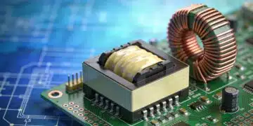
Researchers from SDU Southern Denmark University in Sonderborg, Denmark demonstrated a novel layer-by-layer technique to fabricate nano-scale polypropylene for precise control of nanocomposite capacitor dielectric morphologies in metallized film capacitors.

Nanocomposite dielectrics are an increasingly important area of innovation in capacitor research as an avenue to improve capacitive energy density, electrical breakdown strength, and temperature stability of devices.

RelatedPosts

RF Inductors: Selection and Design Challenges for High-Frequency Circuits

Wk 45 Electronics Supply Chain Digest

Transformer Safety IEC 61558 Standard

In such devices, morphology control is critical in order to optimize electrical field distribution in the device and to prevent the clustering of nanoparticles lowering breakdown voltages. However, this is difficult to achieve with large-scale fabrication techniques, such as melt extrusion and stretching, as melt processing can induce clustering and offers few possibilities for fine structure control of length scales below 1 µm.

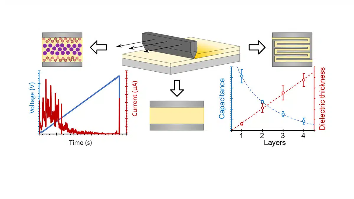
Layer-by-layer fabrication offers a potential bottom-up alternative whereby dielectrics are printed by successive depositions of ultra-thin layers of a room-temperature-stable polymer ink. This would allow fine thickness and morphology control and could easily be adapted to industrial-scale printing techniques, like roll-to-roll slot-die coating. This study explores this technique by developing polypropylene-based inks in industry-friendly solvents that are then used to fabricate capacitor devices. A gel ink was able to be used to deposit ultrathin (sub-200 nm) layers of mostly amorphous polypropylene with high reproducibility.

Capacitors based on these polypropylene layers perform commensurate with commercial devices, exhibiting excellent self-clearing and breakdown performance. Successive depositions of the ink were also demonstrated, allowing the fabrication of devices with finely tuned thicknesses and capacitances, as well as nanocomposite capacitors. This demonstrates the viability of layer-by-layer dielectric printing at large scale and paves the way for commercial ultra-thin conformable polypropylene capacitors, multi-component sandwich nanocomposite capacitors, and multilayer polypropylene capacitors, as well as brand new possibilities in dielectrics research.

Research Highlights

  • A novel technique to fabricate capacitors with nano-scale layer-by-layer printing
  • Polypropylene gel inks were used to successively print layers as thin as 200 nm
  • Layer thickness is easily controllable, and the capacitance is highly predictable
  • Incorporation of BaTiO3 nanoparticles was demonstrated in a structured dielectric
  • Presents pathway to the commercial printing of structured nanocomposite capacitors
Fig. 1. A schematic of the proposed LBL capacitor fabrication process. (1) the process begins with a metal foil (e.g. aluminium) which will serve as bottom electrode and substrate. (2) the first coating of dielectric ink is applied to the metal foil using a high-volume printing technique, such as R2R slot-die coating, which sets to form the first dielectric layer (3). (4) successive coatings are made with the dielectric ink to build up the thickness of the dielectric layer before the top electrode is deposited. Depending on the combinations of inks and the sequence used, designs such as sandwich nanocomposite capacitors (5), ultrathin polypropylene capacitors (6), and multilayer polypropylene capacitors (7) can be printed.

Conclusion

This study detailed the production of room-temperature-stable polypropylene inks in industry-friendly solvents with the goal of demonstrating LBL printing of a polymer dielectric capacitor. The ink was produced by high-temperature emulsification and was gel based – exhibiting no evidence of nanoparticle formation. The ink was able to reproducibly deposit ultra-thin layers of largely amorphous polypropylene, which performs consistent with commercial polypropylene as a dielectric material, particularly with regard to self-clearing capabilities. Furthermore, successive depositions of the gel ink were shown to be possible and to predictably build up the thickness of the dielectric with commensurate changes in the capacitance of the device, and the fabrication of structured nanocomposite capacitors with improved performance was demonstrated.

This study has, therefore, demonstrated a viable new fabrication method for polypropylene-based polymer and nanocomposite capacitors based on a layer-by-layer strategy. Generalisation to other thermoplastic polymers is likely possible, however the self-clearing capability of polypropylene makes it an attractive candidate for continued research. With some optimisation, this technique can be easily scaled to large-scale fabrication via the use of existing commercial printing techniques, allowing the commercialisation of a range of new device structures and fine morphology control in nanocomposite dielectrics. Furthermore, LBL dielectric fabrication can act as a platform for future research to explore a wide variety of different dielectric structures with precision – allowing both confirmation of theoretical models and the development of new dielectric materials.

Full paper can be viewed and downloaded at: https://doi.org/10.1016/j.pedc.2022.100025

Related

Source: Science Direct

Recent Posts

RF Inductors: Selection and Design Challenges for High-Frequency Circuits

10.11.2025
23

Transformer Safety IEC 61558 Standard

7.11.2025
8

ESR of Capacitors, Measurements and Applications

7.11.2025
40

3-Phase EMI Filter Design, Simulation, Calculation and Test

6.11.2025
48
Image credit: Samtec

How to Match the Right Connector with Protocol Requirements

6.11.2025
13

Smoltek CNF-MIM Capacitors Pass 1,000h Reliability Test

6.11.2025
12

Capacitor Lead Times: October 2025

6.11.2025
65

Paumanok Unveils Aluminum Capacitor Foils World Markets Study 2025-2030

6.11.2025
14

Transformer Design Optimization for Power Electronics Applications

4.11.2025
23

Upcoming Events

Nov 11
17:00 - 18:00 CET

Industrial Applications Demand More from Interconnects in Next-Gen Designs

Nov 12
11:00 - 12:00 CET

PCB Design: Impedance is for everyone!

Nov 12
November 12 @ 12:00 - November 13 @ 14:15 EST

Microelectronic Packaging Failure Modes and Analysis

View Calendar

Popular Posts

  • Buck Converter Design and Calculation

    0 shares
    Share 0 Tweet 0
  • Boost Converter Design and Calculation

    0 shares
    Share 0 Tweet 0
  • LLC Resonant Converter Design and Calculation

    0 shares
    Share 0 Tweet 0
  • Flyback Converter Design and Calculation

    0 shares
    Share 0 Tweet 0
  • Ripple Current and its Effects on the Performance of Capacitors

    3 shares
    Share 3 Tweet 0
  • MLCC and Ceramic Capacitors

    0 shares
    Share 0 Tweet 0
  • Dual Active Bridge (DAB) Topology

    0 shares
    Share 0 Tweet 0
  • What is a Dielectric Constant and DF of Plastic Materials?

    4 shares
    Share 4 Tweet 0
  • SEPIC Converter Design and Calculation

    0 shares
    Share 0 Tweet 0
  • Flying Capacitors

    0 shares
    Share 0 Tweet 0

Newsletter Subscription


Passive Components Blog

© EPCI - Leading Passive Components Educational and Information Site

  • Home
  • Privacy Policy
  • EPCI Membership & Advertisement
  • About

No Result
View All Result
  • Home
  • Knowledge Blog
  • PCNS

© EPCI - Leading Passive Components Educational and Information Site

This website uses cookies. By continuing to use this website you are giving consent to cookies being used. Visit our Privacy and Cookie Policy.
Go to mobile version