In this article we will discuss what is a resistor voltage and frequency dependence in basic relations and also specific to the resistor technologies.
Voltage Dependence
If we apply a voltage on a resistor it’s resistance will drop slightly in certain types. Therefore the resistance change is negative. The change per volt of applied voltage is called voltage coefficient, VC, and is expressed in %/V or better, μV/V. The coefficient is determined not only by the resistive material but also by the dimensions, i.e., the electrical field strength, and the time of applied voltage. Thus, MIL-STD-202, Method 309 prescribes measurements when the voltage is applied intermittently for less than 0.5 seconds. Two measurements is performed: the resistance (r) at 0.1 x rated voltage (VR) and the resistance (R) at 1.0 x VR. The voltage coefficient, VC, then is computed as:

If we disregard pure metallic resistive elements common values of the voltage coefficient are between –10 and –100 μV/V. The voltage dependence is negligible for resistance values below 1000 ohms.
An evident voltage dependence combined with AC voltages will cause distortion and a third harmonic attenuation.
Frequency Dependence
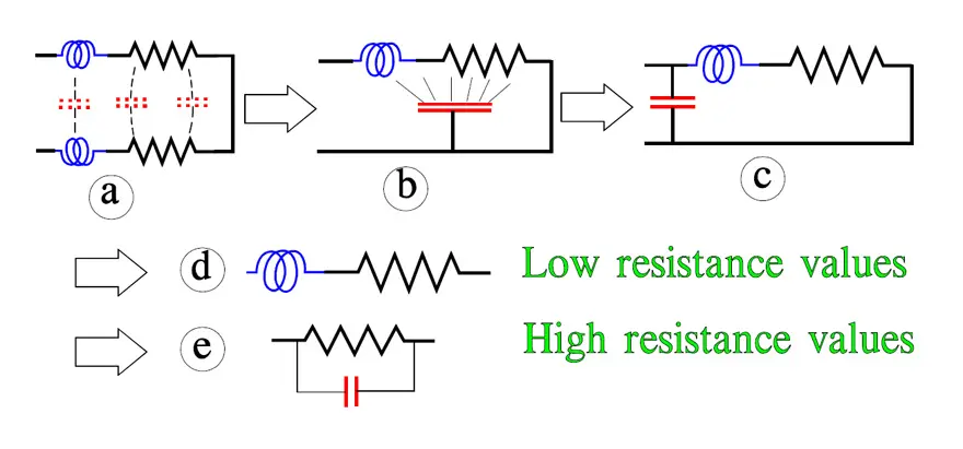
A resistor has a certain parasitic degree of both capacitance and inductance. Between the turns there is a certain capacitive connection. Inductance appears already in a straight lead, approximately 1 nH/mm of length but is amplified by the coil action from windings and spiraled patterns. In carbon composition resistors only capacitance emanating from the multitude of parallel current paths manifests itself.
Figure 1. shows the equivalent circuit being simplified to models for high and low resistance values.
- a) Small sizes
- b) low R-value
- c) Chip design
- d) Small or no lead wire (SMD)
- e) Even body
The frequency dependence of resistance decreases if the resistors:
- have small dimensions.
- have a low resistance value.
- are of a thin film design. Even a thick film design is favorable.
- have as short a lead as possible, like SMDs.
- are geometrically even, i.e., without sudden geometrical changes along the resistor body.
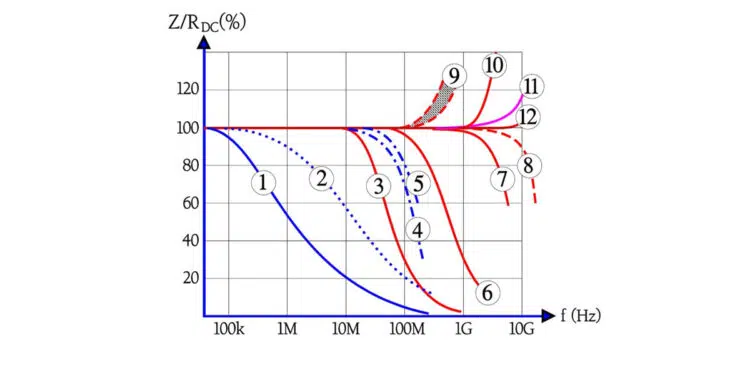
How the frequency dependence may influence the impedance is shown in Figure 2.
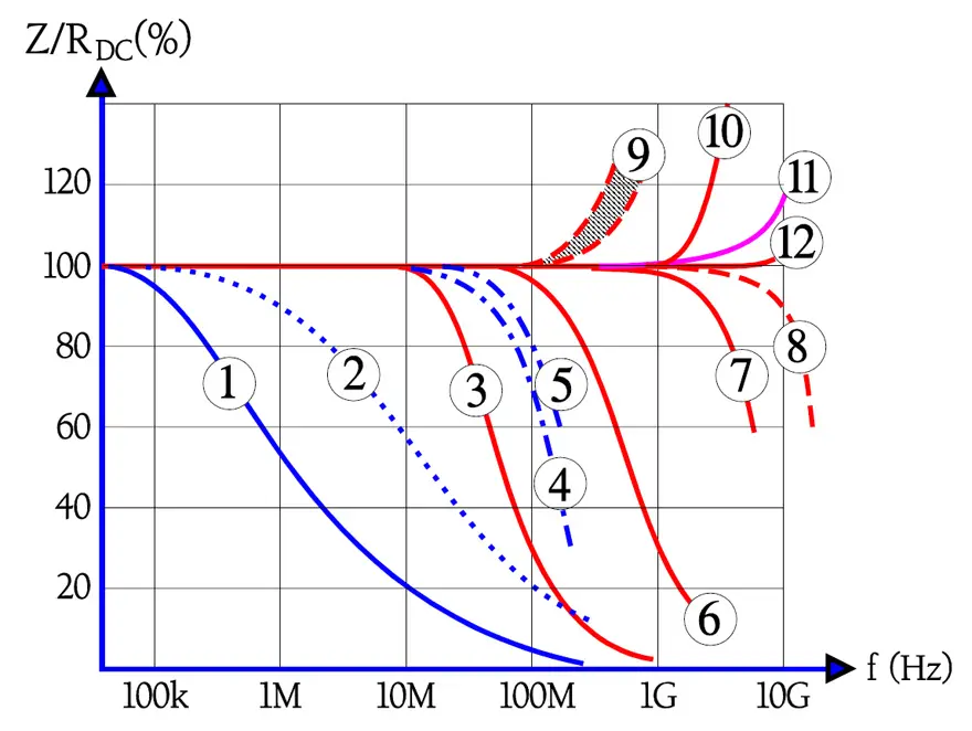
- Carbon composition, ¼ W, 1 MW.
- Carbon composition, ¼ W, 100 kW.
- Chip, thick film, EIA size 0603, 100 kW; c » 0.05 pF; L » 0.4 nH.
- Metal glaze or metal film, DIN size 0207, 100 kW; c » 0.4 pF.
- MELF, DIN size 0204, 10 kW.
- Chip, thick film, EIA size 0603, 10 kW; c » 0.05 pF; L » 0.4 nH.; Chip, metal foil, EIA size 1210, 10 kW.
- Chip, thick film, EIA size 0603, 1 kW; c » 0.05 pF; L » 0.4 nH.
- MELF, DIN size 0102, high frequency design, 10 W; c » 0.035 pF; L » 0.8 nH.
- MELF, DIN size 0204, 10 W.
- Chip, thick film, EIA size 0603, 10 W; c » 0.05 pF; L » 0.4 nH.
- Chip, thin film, EIA size 0603, 100 W; c » 0.035 pF; L » 1.2 nH.
- Chip, thick film, EIA size 0603, 100 W; c » 0.05 pF; L » 0.4 nH.
The examples in Figure 2. represent a guide only. They are taken from major manufacturers’ data sheet. Note how the resistance value of an otherwise equivalent component influences the parameters: No. 3, 6, 7, 10 and 12. Another example, No. 8, shows a MELF component that, by means of a specific spiraling technique, is given excellent high frequency characteristics. Generally the frequency dependence of the different resistor materials can be divided into three groups:
| Technology | Frequency Dependence |
| Carbon composition | high |
| Metal glaze, cermet, thick film | moderate to low |
| Metal film, metal oxide and carbon film | low |
Film resistors may approximately be classified as follows:
- values < 100Ω are inductive.
- values between 100 and 470Ω are practically true resistive.
- values above 470Ω are capacitive.
Thin Film Chip High Frequency Resistors
As the industry extends products above the GHz range (5G), an understanding and improvement of resistors especially in thin films products’ performance needs to be considered.
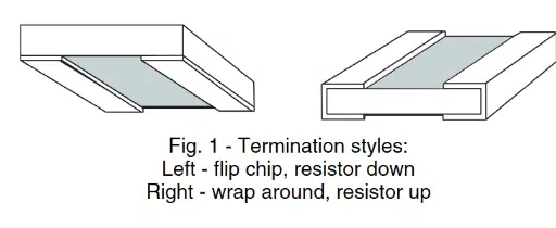
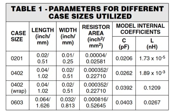
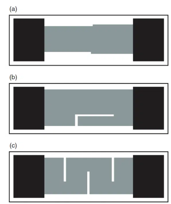
Performance of thin film resistors at high frequency is dependent on the case size, trim method, part value and termination style. The reduction in parasitic impedance for smaller cases sizes is consistent with the smaller landing pads and device dimension.
Termination style:
The large change between 0201 and the 0402 and 0603 can be related to significant reduction in maximum resistor area. The ratios of the maximum areas for the resistors by case size (0603 : 0402 : 0201) are 1 : 2.32 : 20.4. The small change in device area for the 0402 and 0603 case sizes is most likely related to the small differences and occasional reversal in the device performance.
Trim method:


