





Common-mode noise from isolated power modules and digital isolators can be diverted past the measurement network with a capacitor across the isolation barrier, and this capacitor can be built from overlapping copper planes in the printed circuit board instead of a discrete Y capacitor. This article explains how common-mode current flows in an isolated DC/DC design, how to calculate the required bridge capacitance and how to implement it as a PCB stitching capacitor, for design engineers who want to pass conducted emission limits with fewer components.
The webinar by Würth Elektronik, presented by Timur Uludag, product manager of the MagI³C power module division, discusses strategies for reducing the bill of materials (BOM) while improving common-mode noise reduction [1], [2]. It introduces a method to design compliant filters for power modules and digital isolators without relying on discrete Y safety capacitors, and compares two-layer and four-layer evaluation board layouts with integrated capacitances from about 14 pF to 1,400 pF. The article adds the calculation method from the related application note [3] and recalculates the published examples.
Key Takeaways
- In isolated DC/DC converters, common-mode noise dominates: the switching node drives current through the interwinding capacitance of the transformer, and the current returns through stray capacitance to earth and through the LISN.
- A bridge (Y) capacitor between primary and secondary ground gives the noise current a low-impedance loop around the module, so less current reaches the LISN.
- The attenuation follows from a capacitive voltage divider; the short rule of thumb, attenuation = 20·log(CY/CK), is valid only when the bridge capacitance is much larger than the stray capacitance to the environment.
- Overlapping primary and secondary ground planes form a stitching capacitor: about 130 pF on a two-layer 80 × 80 mm board and about 920 pF to 1,400 pF on a four-layer board, measured as equivalent to discrete capacitors of similar value.
- A stitching capacitor removes a safety-rated part from the BOM and has very low inductance, but its value is fixed by the layout and must be planned from the start together with creepage, clearance and insulation requirements.
- Beyond a certain value, more capacitance brings little benefit: the 1,400 pF layout performed nearly the same as the 920 pF layout.
Webinar Outline
The webinar runs about 38 minutes, including questions and answers. The presentation is divided into four parts:
- EMI basics: differential-mode and common-mode noise, parasitic capacitance and the function of a Y capacitor.
- EMI performance of realized power module PCB layouts with discrete and integrated Y capacitors.
- Optimized digital isolator layouts with stitching capacitors.
- Würth Elektronik design examples and support for the layout design.
Common-Mode Noise in Isolated Power Modules
Isolated and non-isolated converters generate different noise mixtures. Understanding the noise path in an isolated module explains why a single capacitor across the barrier can be more effective than a common mode choke.
Differential Mode and Common Mode
Differential-mode current flows in the supply lines in opposite directions; it is essentially the switched input current of the module and dominates in non-isolated converters such as buck regulators. Common-mode current flows in the same direction on both supply lines; it is caused mainly by the high dv/dt of the switching elements and dominates in isolated power modules [2], [3].
In an isolated module, the switched primary voltage drives a noise current INOISE through the interwinding capacitance CK of the transformer to the secondary side. The current travels along the output lines, flows through the coupling capacitance CP of the board, cables and load to the ground reference and closes its loop through the LISN on the input side [3]. The input and output lines also act as antennas, so part of this current is radiated. The mechanism is the same as in the demonstration in EMI noise on data cables caused by an isolated power module.
Parasitic Capacitances
Parasitic capacitance exists between any two conductors at different potentials, for example two parallel planes or a conductor above a flat surface [2]. Its reactance XC at frequency f falls with increasing capacitance C, Eq. (1) [3]:
Because all elements in the common-mode loop are capacitive, the noise current rises with frequency. For the 80 × 80 mm evaluation board with 100 cm output cables placed 40 cm above the ground plate, the coupling capacitance CP was measured by inserting two 15 µH inductors in the input lines, which form a series resonant circuit with CP. With the parallel inductance L = 7.5 µH and the resonance fres ≈ 15 MHz seen in the emission plot, Eq. (2) gives CP ≈ 15 pF [3]:
CP depends strongly on the distance to the ground reference and on the cable length, so it changes from one application to another. For this reason the webinar uses a standardized set-up based on CISPR 16-2-1, with the LISN, EMI receiver, power supply, load and the device under test at defined positions, as a reproducible reference [2], [4]. The set-up, limits and detectors are described in passing conducted emissions using line filters.
Bridge Capacitor: Keeping Noise Away from the LISN
There are three general ways to pass a conducted emission test: suppress the noise inside the module, keep the noise current away from the LISN, or attenuate it so that the remaining voltage at the LISN is below the limit. The bridge capacitor uses the second approach.
A capacitor CY between the primary and the secondary side creates a second loop for INOISE. If this loop has a lower impedance than the path through CP, earth and the LISN, most of the noise current circulates within the module and its bridge capacitor and does not reach the LISN [2], [3]. A capacitor is the natural component for this branch, because its impedance decreases with frequency like that of the noise source path, and it keeps the DC isolation. The input and output capacitors of the module balance the common-mode currents between the two lines of each side, so one bridge capacitor is sufficient instead of two [3].
EMC Meets Kirchhoff’s Law
The attenuation follows from comparing the voltage across the LISN without and with the bridge capacitor. With the common-mode source voltage VS, the LISN impedance ZV, the impedance of the interwinding capacitance ZK and the impedance of the coupling capacitance ZP, the LISN voltage without the bridge capacitor is given by Eq. (3) [3], [2]:
With the bridge capacitor of impedance ZY in parallel with the series connection of ZP and ZV, the LISN voltage becomes Eq. (4):
The ratio A = V2/V1, expressed in decibels as a = 20·log10(A), is the attenuation provided by the bridge capacitor. Combining Eq. (3) and Eq. (4) gives the full expression Eq. (5) [3]:
Rule of Thumb and Its Limits
If the bridge capacitor is much larger than the coupling capacitance, so that ZY is much smaller than ZP, and the LISN impedance of about 25 Ω for common mode is negligible compared with the capacitive reactances, the expression simplifies to the ratio of the two capacitances, Eq. (6) [3]:
Solving for the bridge capacitance gives the design equation Eq. (7), where a is the required attenuation in decibels as a negative number:
Because all impedances in the model are capacitive and ZV is small, the predicted attenuation is nearly independent of frequency. In practice, the bridge capacitor cannot keep the noise current out over the whole 150 kHz to 30 MHz range: below a few megahertz the emissions of an isolated module are usually dominated by differential-mode noise, which the bridge capacitor does not affect, and at high frequencies the inductance of the capacitor and its connections limits the bypass [3]. The short formula should only be used when CY is much larger than CP; otherwise the full expression Eq. (5) must be used.
Worked Example from the Application Note
For an SIP-4 power module with 12 V input and 5 V / 200 mA output, the emissions between 4 MHz and 30 MHz were common-mode dominated, and 15 dB of attenuation was targeted for the 20 MHz to 30 MHz range. With the datasheet isolation capacitance of 75 pF as CK, Eq. (7) gives 75 pF / 0.178 = 422 pF, and the standard value 470 pF was chosen [3].
Recalculated with the short formula, 470 pF and 75 pF give 15.9 dB. The full expression at 10 MHz with CP = 20 pF and ZV = 25 Ω gives 15.5 dB, which confirms that the simplification is acceptable in this case. The measurement showed almost 19 dB. The application note explains the higher measured value mainly by the actual interwinding capacitance of about 60 pF, below the specified maximum of 75 pF; with 60 pF the short formula gives 17.9 dB. Measurement uncertainty, model simplifications and component tolerances add to the difference. The datasheet value of CK is a worst-case maximum, so a design based on it tends to be conservative.
When the Rule of Thumb Fails
Small modules with low interwinding capacitance show the limit of the short formula. The MagI³C-FIMM module used in the webinar has a typical parasitic coupling capacitance of only 8 pF [2], [5], which is smaller than the coupling capacitance CP of 15 pF to 20 pF of the test set-up. For a target of 20 dB, the short formula suggests CY = 8 pF × 10 = 80 pF. The full expression Eq. (5) with CP = 15 pF gives only 13 dB for 80 pF and requires about 220 pF for 20 dB. In such cases, the full expression or a measurement is needed to choose the starting value.
PCB Stitching Capacitor
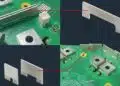
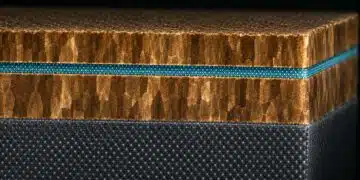
A capacitor across the isolation barrier does not have to be a discrete component. Any overlap of copper areas connected to primary and secondary ground forms a capacitor.
Calculating the Stitching Capacitance
The stitching capacitance C of two overlapping planes is the parallel-plate capacitance of the overlap area A = l·w, with length l and width w, separated by an insulating PCB layer of thickness d with relative permittivity εr, Eq. (8) [2]:
Here ε0 = 8.854 pF/m is the permittivity of free space. In a multilayer board, each pair of adjacent planes at alternating potentials forms its own capacitor, and these capacitors add in parallel. Thin dielectric layers and many overlapping layers increase the capacitance per area [6]. Table 1 shows the capacitance per square centimetre for typical layer thicknesses, assuming FR-4 with εr ≈ 4.4.
| Dielectric thickness d | Capacitance per area | Area for 470 pF |
|---|---|---|
| 1.5 mm (two-layer core) | 2.6 pF/cm² | 181 cm² |
| 0.71 mm | 5.5 pF/cm² | 86 cm² |
| 0.38 mm | 10.3 pF/cm² | 46 cm² |
| 0.2 mm | 19.5 pF/cm² | 24 cm² |
| 0.14 mm | 27.8 pF/cm² | 17 cm² |
| 4-layer stack 0.38 / 0.71 / 0.38 mm, alternating grounds | 26.0 pF/cm² | 18 cm² |
The table explains the layout results. An 80 × 80 mm board has 64 cm², so a two-layer board with a 1.5 mm core can provide at most about 165 pF even with full overlap. The 470 pF used on the evaluation board therefore requires either a discrete capacitor or a four-layer stack-up with thin dielectrics.
Stitching Capacitance and Insulation
The stitching capacitor has the same function as a discrete Y capacitor but uses the PCB laminate as its dielectric. The insulation between the overlapping planes becomes part of the isolation barrier, and depending on the design the stitching capacitor can be implemented for functional, basic or reinforced insulation [1], [2]. The surface creepage and clearance distances between the primary and secondary copper must remain at least equal to those of the module, while the overlapping planes are placed on inner layers or on opposite sides of the board. The distance through insulation and the electric strength of the laminate must meet the applicable insulation standard; the selection of isolation methods and the related standards are summarized in galvanic isolation methods, standards and implementation and in [7].
Compared with a discrete high-voltage capacitor, the plane capacitor has extremely low inductance and its capacitance is distributed over a large area, which keeps it effective up to high frequencies [8]. Large barrier capacitance also increases the AC leakage current and the coupling of fast common-mode transients between the two sides, which can be unacceptable in medical or other low-leakage applications.
Power Module Layouts Compared
The webinar compared four layouts of an 80 × 80 mm evaluation board for the MagI³C-FIMM power module, a 1 W isolated module in a 9 × 7 × 3.1 mm LGA-7 package with integrated input and output capacitors, functional isolation and EN 55032 Class B performance [2], [5]. The differential-mode input filter and the output capacitor were populated in all versions, so that the comparison focuses on common-mode noise. Boards with more than four layers were not considered.
- Version 1, two layers without a Y capacitor: secondary ground on the top layer and primary ground on the bottom layer, 1.5 mm apart, with a small unintentional overlap of about 14 pF. The emissions came close to the Class B limit, which was judged not sufficient.
- Version 2, two layers with an integrated Y capacitor: primary and secondary ground areas overlap as much as possible while keeping the creepage distances of the module, giving about 130 pF. The measured improvement was about 10 dB; the calculation predicted about 12 dB.
- Version 3, four layers: primary and secondary ground areas on all layers, with dielectric thicknesses of about 0.38 mm, 0.71 mm and 0.38 mm, form several parallel capacitors totalling about 920 pF. The calculated attenuation for this value range was about 28 dB.
- Version 4, four layers with maximum capacitance: the top layer is fully secondary ground and the bottom layer fully primary ground, giving about 1,400 pF. The emissions were nearly the same as with Version 3.
In direct comparisons, a 100 pF discrete capacitor on the two-layer board gave practically the same result as the 130 pF integrated capacitor, and a 1,000 pF discrete capacitor gave nearly the same result as the 920 pF four-layer layout [2], [1]. The integrated and discrete versions are therefore interchangeable when their values are similar.
| Version | Construction | Capacitance | Calculated attenuation vs 14 pF | Measured result |
|---|---|---|---|---|
| 1 | Two layers, no intended Y capacitor | ≈ 14 pF | Reference | Not enough margin |
| 2 | Two layers, integrated | ≈ 130 pF | 12.3 dB | ≈ 10 dB, good |
| Discrete | Two layers, discrete capacitor | 100 pF | 10.4 dB | ≈ same as Version 2 |
| Eval board | Two layers, discrete capacitor | 470 pF | 22.5 dB | ≈ 20 dB, enough margin |
| 3 | Four layers, integrated | ≈ 920 pF | 28.1 dB | Better |
| Discrete | Two layers, discrete capacitor | 1,000 pF | 28.8 dB | ≈ same as Version 3 |
| 4 | Four layers, maximum overlap | ≈ 1,400 pF | 31.7 dB | ≈ same as Version 3 |
The recalculated values with the full expression reproduce the trend of the measurements: about 12 dB for 130 pF and about 28 dB for 1,000 pF. The model predicts a further 3.6 dB from 920 pF to 1,400 pF, but the measurement showed almost no difference. At this point the remaining emissions are no longer limited by the bridge capacitance but by other paths, such as differential-mode noise, the inductance of the connections and the noise floor of the set-up. Beyond about 1 nF, more capacitance mainly adds layout effort and barrier capacitance.
The evaluation board itself uses the two-layer layout with a discrete 470 pF Y capacitor. The webinar explained that this gives enough margin and allows users to replace the capacitor, for example with 100 pF, 470 pF or 1 nF, to test the performance needed in their application [1]. Würth Elektronik provides layout recommendations with the stitching capacitor configuration in the module datasheets and design examples [2].
Discrete or Stitching Y Capacitor
| Aspect | Stitching capacitor | Discrete Y capacitor |
|---|---|---|
| BOM and cost | No additional part to buy, place or store | Safety-rated part in the BOM |
| Availability | Always present as part of the layout | Can be changed or removed during tests |
| Insulation | Distances defined by the PCB; reinforced insulation can be realized | Component rating and placement must meet the insulation requirements |
| High-frequency behaviour | Very low inductance, distributed capacitance | Lead and package inductance limit the self-resonant frequency |
| Design flexibility | Value fixed; change requires a new layout | Value changed by replacing the part |
| Design effort | Must be planned from the start; easier on four layers | Simple to add late in the design |
Digital Isolator Layouts
Digital isolators with integrated isolated power converters face the same common-mode mechanism, often at higher switching frequencies. The Würth Elektronik digital isolators include the WPME-CDIP family, a four-channel capacitive digital isolator with an integrated 0.65 W isolated DC/DC converter, data rates up to 100 Mbps and reinforced insulation up to 5 kV RMS [9].
A four-layer 80 × 80 mm board with about 600 pF of integrated capacitance, using a 140 µm dielectric between primary and secondary ground planes, kept both conducted and radiated emissions well below the limits, with ample margin to Class A [2], [1].
A more complex reference design, a potential-free voltage measurement for a battery in a station battery compartment, transmits the measured signal through a digital isolator and a twisted-pair cable to the operator. The four-layer receiver board, about 77 × 50 mm, forms about 1 nF between primary and secondary ground on the bottom and internal layers. Compared with an unfiltered two-layer version, the emissions dropped and left sufficient margin to Class B [2], [1]. The presenter noted that a four-layer design with the required capacitance and via arrangement takes experience.
Independent application notes for isolators with integrated power report the same effect: interplane stitching capacitance across the barrier was the most effective single measure, reducing radiated peaks by 25 dB to 30 dB, and is most effective when its inductance is low and it extends along the whole length of the barrier [8].
Layout Guidelines for Stitching Capacitors
The guidelines below combine the webinar results with general PCB practice for isolation barriers [2], [8], [6]. General layout rules for EMC are covered in EMC-compliant PCB and connector design guidelines.
- Plan the stitching capacitor at the start of the layout, when the stack-up and the ground areas are defined.
- Estimate CK from the module datasheet and CP from the set-up, then calculate the target CY with the full expression when CY is not much larger than CP.
- Use four layers when more than about 150 pF is needed on a small board, and use thin dielectrics between the overlapping planes.
- Alternate primary and secondary ground on adjacent layers to add several capacitors in parallel.
- Keep the overlap close to the module or isolator and along the full length of the barrier to minimize inductance.
- Maintain the required surface creepage and clearance, and verify the distance through insulation and the dielectric strength of the laminate for the required insulation class.
- Leave footprint space for an optional discrete Y capacitor in prototypes, so that the value can be tuned during pre-compliance tests.
- Check leakage-current and transient-coupling limits before adding large barrier capacitance in medical and other low-leakage applications.
Design Checklist
The checklist summarizes the parameters to compare when common-mode noise of an isolated module must be reduced with a bridge capacitor.
- Noise mode: confirm that the failing frequencies are common-mode dominated, typically above a few megahertz for small isolated modules.
- Required attenuation: margin to the limit plus a safety margin in the relevant frequency range.
- Interwinding capacitance CK: from the module datasheet, usually specified as a maximum.
- Coupling capacitance CP: estimated from the set-up geometry or measured by series resonance.
- Bridge capacitance CY: from Eq. (7) when CY ≫ CP, otherwise from Eq. (5).
- Implementation: stitching capacitor from the stack-up with Eq. (8), or a discrete Y1 or Y2 capacitor with the required rating.
- Insulation: functional, basic or reinforced; creepage, clearance and distance through insulation.
- Verification: conducted and radiated emissions in the final set-up, as CP changes with cables, enclosure and mounting.
Conclusion
Common-mode noise in isolated power modules and digital isolators follows a predictable capacitive path through the transformer interwinding capacitance, the stray capacitance to earth and the LISN. A bridge capacitor across the barrier diverts this current, and its value can be calculated from a simple voltage-divider model, as long as the limits of the short rule of thumb are respected.
The webinar measurements show that a stitching capacitor formed by overlapping ground planes performs like a discrete Y capacitor of similar value. On a four-layer board, several hundred picofarads to more than 1 nF are available without an additional component, which reduces the BOM and simplifies insulation, provided the capacitor is planned from the start of the layout.
FAQ
In an isolated module, the switching node drives current through the interwinding capacitance of the transformer to the secondary side. This current returns through the stray capacitance of the board, cables and load to earth and through the LISN, so it appears as common-mode noise. Non-isolated converters have no such path and are dominated by differential-mode noise from the switched input current.
A bridge capacitor, also called a Y capacitor, connects the primary and secondary side of the isolated converter. It gives the common-mode noise current a low-impedance loop around the module, so most of the current circulates locally instead of flowing through earth and the LISN. The voltage measured at the LISN falls, which reduces conducted emissions without a common mode choke.
The rule of thumb sets the attenuation equal to 20 times the logarithm of the ratio of the transformer interwinding capacitance to the bridge capacitance. For 15 dB with 75 pF interwinding capacitance, this gives about 420 pF, rounded to 470 pF. The simplification is valid only when the bridge capacitor is much larger than the stray capacitance to the environment.
The short formula assumes that the bridge capacitor is much larger than the coupling capacitance of the set-up to earth. Small modules may have an interwinding capacitance of only about 8 pF, lower than a typical coupling capacitance of 15 to 20 pF. Then the short formula underestimates the required value, and the full voltage-divider expression or a measurement must be used.
A PCB stitching capacitor is formed by overlapping copper planes connected to primary and secondary ground, separated by the insulating laminate of the board. Its capacitance follows the parallel-plate formula and grows with the overlap area and with thinner dielectrics. Several overlapping layers add in parallel, so a four-layer board can provide hundreds of picofarads to more than one nanofarad.
Yes, if it provides a similar capacitance and meets the insulation requirements. In the webinar measurements, a 130 pF integrated capacitor performed like a 100 pF discrete capacitor, and a 920 pF four-layer layout performed like a 1,000 pF discrete capacitor. The stitching capacitor removes a safety part from the BOM but cannot be changed without a new layout.
No. In the webinar, increasing the integrated capacitance from about 920 pF to 1,400 pF on a four-layer board brought nearly no further improvement. Once the bridge path is dominant, the remaining emissions are set by other mechanisms, such as differential-mode noise, connection inductance and the measurement set-up. Additional capacitance then mainly increases layout effort and barrier capacitance.
According to the webinar, stitching capacitors can be designed for functional, basic and reinforced insulation. The surface creepage and clearance distances must be kept, and the laminate between the overlapping planes must meet the required distance through insulation and electric strength. The applicable safety standard of the end product defines these requirements.
How to Reduce Common-Mode Noise with a Stitching Capacitor
Step-by-step procedure for reducing common-mode noise of an isolated power module or digital isolator with a bridge capacitor implemented as a PCB stitching capacitor.
- Identify the common-mode range
Measure the conducted emissions of the isolated module and identify the frequency range in which common-mode noise exceeds the limit, typically above a few megahertz.
- Define the required attenuation
Subtract the limit from the measured level in that range and add a safety margin to obtain the required attenuation in decibels.
- Collect the capacitances
Take the interwinding capacitance from the module datasheet and estimate the coupling capacitance to earth from the set-up geometry or a series-resonance measurement.
- Calculate the bridge capacitance
Use the rule of thumb when the bridge capacitor will be much larger than the coupling capacitance; otherwise use the full voltage-divider expression.
- Choose the implementation
Decide between a discrete safety-rated Y capacitor and a PCB stitching capacitor, and calculate the overlap area for the chosen stack-up with the parallel-plate formula.
- Lay out the stitching capacitor
Overlap primary and secondary ground on alternating layers close to the module and along the barrier while keeping creepage, clearance and insulation requirements.
- Verify by measurement
Repeat the conducted and radiated emission measurements in the final set-up and adjust the capacitance with an optional discrete capacitor if needed.
Further Reading
- Common Mode Noise Mitigation: further methods for common-mode suppression.
- Why Isolated DC/DC Power Supplies Fail Late: reliability aspects of isolated converters.
- Overvoltage and Transient Protection for DC/DC Power Modules: protection of the module input.
- Introduction to EMI Filtering: filter configurations and insertion loss.
- EMC Filters Explained: From Component to Design: choosing filter components.
- Transformer Testing: Parasitic Inductance and Capacitance: measuring the interwinding capacitance.
- DC/DC Push-Pull Converter vs PSFB Design Guide: isolated topologies used in power modules.
References
- Decreasing the BOM and Improving Common Mode Noise Reduction – webinar recording, Würth Elektronik, 2024.
- T. Uludag, Decreasing the BOM and Improving Common Mode Noise Reduction – webinar slides, Würth Elektronik eiSos, 2024.
- T. Uludag, ANS022 Bridge Capacitor for Isolated Power Modules, the Whole Truth, No Myths, Würth Elektronik eiSos, application note, 2025.
- A. Stirn, SN023 Conducted Emissions Test, Würth Elektronik eiSos, support note, 2024.
- MagI³C-FIMM Fixed Isolated MicroModule – product page, Würth Elektronik eiSos.
- Minimizing Radiated Emissions from Multiple isoPower Devices in Dense PCB Layouts, Analog Devices, technical article.
- ANP151 Mastering Galvanic Isolation: Ensuring Safety in High-Power Electronics with Würth Elektronik Products, Würth Elektronik eiSos, application note, 2025.
- M. Cantrell, AN-0971 Recommendations for Control of Radiated Emissions with isoPower Devices, Analog Devices, application note.
- WPME-CDIP Capacitive Digital Isolator Powered – product page, Würth Elektronik eiSos.
- Würth Elektronik – EPCI premium supplier page, Passive Components Blog.
Article revised and technically reviewed in November 2026: expanded the webinar announcement into a technical summary with the common-mode noise path, the bridge capacitor calculation and its limits, PCB stitching capacitor design, recalculated layout comparisons for power modules and digital isolators, layout guidelines, checklist, FAQ and How-to, and added referenced sources.