source: Nanowerk news
In trying to bring brain-like (neuromorphic) computing closer to reality, researchers have been working on the development of memory resistors, or memristors, which are resistors in a circuit that ‘remember’ their state even if you lose power.
Today, most computers use random access memory (RAM), which moves very quickly as a user works but does not retain unsaved data if power is lost. Flash drives, on the other hand, store information when they are not powered but work much slower. Memristors could provide a memory that is the best of both worlds: fast and reliable.
“Previously there was a work by Mark Hersam’s group on memristor effect in monolayer MoS2 in a planar configuration, Deji Akinwande, an Associate Professor at the University of Texas at Austin, tells Nanowerk. “This prior work has inspired us to consider vertical sandwich structures for memristors because of the massively higher density and scalability. However, everyone we consulted doubted such an effect could be possible in a vertical configuration because the active layer spacing between metal electrodes is less than 1 nanometer, so leakage current will kill the device.”
In new work, published in Nano Letters (“Atomristor: Nonvolatile Resistance Switching in Atomic Sheets of Transition Metal Dichalcogenides”), Akinwande and his team discovered non-volatile memory effect in atomically thin 2D materials such as MoS2. This effect is similar to memristors or RRAM in metal oxide materials. This experimental work is supported by preliminary calculations.
These devices can be collectively labeled atomristor, in essence, memristor effect in atomically thin nanomaterials or atomic sheets. Because MoS2 and related materials are crystalline and have a good electronic barrier prevent current flowing, it is possible to realize working atomristors.
“It had been a conventional belief that you could not scale the memory layer below ∼5nm,” says Akinwande. “Our work overturns this thinking and demonstrates that materials as thin as 0.7nm can afford memory effect.”
The team’s work features the thinnest memory devices and it appears to be a universal effect available in all semiconducting 2D monolayers.
The scientists explain that the unexpected discovery of nonvolatile resistance switching (NVRS) in monolayer transitional metal dichalcogenides (MoS2, MoSe2, WS2, WSe2) is likely due to the inherent layered crystalline nature that produces sharp interfaces and clean tunnel barriers. This prevents excessive leakage and affords stable phenomenon so that NVRS can be used for existing memory and computing applications.
“Our work opens up a new field of research in exploiting defects at the atomic scale, and can advance existing applications such as future generation high density storage, and 3D cross-bar networks for neuromorphic memory computing,” notes Akinwande. “We also discovered a completely new application, which is non-volatile switching for radio-frequency (RF) communication systems. This is a rapidly emerging field because of the massive growth in wireless technologies and the need for very low-power switches. Our devices consume no static power, an important feature for battery life in mobile communication systems.”
Notwithstanding the team’s discovery, there remain fundamental questions regarding mechanisms of NVRS in single-layer atomic sheets. Hence, they are working with theorists and material scientists to elucidate the detailed physics at the atomic level.
“From a scientific view, the biggest challenge is a detailed understanding of the physics,” Akinwande concludes. “From an application point of view, the biggest challenge for maximum performance is to improve the endurance from ∼100 cycles today to more than a million cycles.”
A detailed technical paper by Univeristy of Texas-Austin is available here.
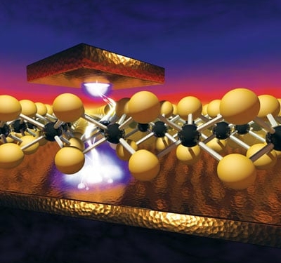
featured image: illustration of electric-field induced memristor effect in single layer MoS2. (Image: Deji Akinwande, University of Texas-Austin)


