Passive Components Blog
No Result
View All Result
  • Home
  • NewsFilter
    • All
    • Aerospace & Defence
    • Antenna
    • Applications
    • Automotive
    • Capacitors
    • Circuit Protection Devices
    • electro-mechanical news
    • Filters
    • Fuses
    • Inductors
    • Industrial
    • Integrated Passives
    • inter-connect news
    • Market & Supply Chain
    • Market Insights
    • Medical
    • Modelling and Simulation
    • New Materials & Supply
    • New Technologies
    • Non-linear Passives
    • Oscillators
    • Passive Sensors News
    • Resistors
    • RF & Microwave
    • Telecommunication
    • Weekly Digest

    KYOCERA AVX Expands Stacked MLCC Capacitors Offering

    Murata and QuantumScape Joint Development for Solid Batteries Ceramic Separators

    YAGEO Unveils Compact 3.6kW LLC Transformer for OBC EV Charging

    Over-Voltage Protection Clippers, Clampers, Snubbers, DC Restorers

    KYOCERA Releases Shielded Board-to-Board Connectors for Reliable EMI Protection

    Wk 41 Electronics Supply Chain Digest

    Samtec Expands Connector Severe Environment Testing Offering

    Silicon Capacitors Market: Shaping the Foundation for Next-Gen Miniaturization Electronics

    YAGEO Releases Compact Coupled Inductors for High-Density VR Designs

    Trending Tags

    • Ripple Current
    • RF
    • Leakage Current
    • Tantalum vs Ceramic
    • Snubber
    • Low ESR
    • Feedthrough
    • Derating
    • Dielectric Constant
    • New Products
    • Market Reports
  • VideoFilter
    • All
    • Antenna videos
    • Capacitor videos
    • Circuit Protection Video
    • Filter videos
    • Fuse videos
    • Inductor videos
    • Inter-Connect Video
    • Non-linear passives videos
    • Oscillator videos
    • Passive sensors videos
    • Resistor videos

    Connector PCB Design Challenges

    Efficient Power Converters: Duty Cycle vs Conduction Losses

    Ripple Steering in Coupled Inductors: SEPIC Case

    SEPIC Converter with Coupled and Uncoupled Inductors

    Coupled Inductors in SEPIC versus Flyback Converters

    Non-Linear MLCC Class II Capacitor Measurements Challenges

    Percolation Phenomenon and Reliability of Molded Power Inductors in DC/DC converters

    Root Causes and Effects of DC Bias and AC in Ceramic Capacitors

    How to Calculate the Output Capacitor for a Switching Power Supply

    Trending Tags

    • Capacitors explained
    • Inductors explained
    • Resistors explained
    • Filters explained
    • Application Video Guidelines
    • EMC
    • New Products
    • Ripple Current
    • Simulation
    • Tantalum vs Ceramic
  • Knowledge Blog
  • Suppliers
    • Who is Who
  • PCNS
    • PCNS 2025
    • PCNS 2023
    • PCNS 2021
    • PCNS 2019
    • PCNS 2017
  • Events
No Result
View All Result
Passive Components Blog
No Result
View All Result

Does NiPdAu Terminations Need Degolding Prior Sn/Pb Soldering ?

10.1.2020
Reading Time: 3 mins read
A A

The use of gold (Au) finish on military and space qualified parts provides useful protection to the base material of leads during storage of the parts. The use of a gold layer over the barrier metal on the lead avoids the appearance of corrosion. On the other hand, as gold is not essentially soluble in Sn nor Pb, embrittlement on the lead can be produced when soldering using SnPb solder.

If the gold layer does not completely dissolve into the solder, then slow intermetallic reactions can proceed in the solid state. The gold reacts with the soldering, forming brittle intermetallics and preferential cleavage planes.

RelatedPosts

KYOCERA AVX Expands Stacked MLCC Capacitors Offering

Murata and QuantumScape Joint Development for Solid Batteries Ceramic Separators

YAGEO Unveils Compact 3.6kW LLC Transformer for OBC EV Charging

For this reason, Military/Aerospace and some levels of industrial standards specify the removal of gold plating from components before they are soldered to the PCB to try and inhibit the formation of this gold inter-metallic and the higher percentage risk of fractures forming in the solder joint during end use, especially where the PCB’s are destined for harsh environments. To eliminate the risk, the safest option is to remove the gold before assembly, this process is called “degolding” and it is addressed by the standard J-STD-001 “Requirements for Soldered Electrical and Electronic Assemblies” in the paragraph “Gold removal”

During year 2001, all the NiPd finished packages from manufacturer Texas Instruments were substituted by NiPdAu finished ones (both known as Pre-Plated finishes, PPF, in which the solderable finish is applied at the leadframe maker, not in a post mold finishing operation, PMF), which would provide a barrier to degradation of the finish. This finish consists on three layers over the copper base metal: a first one of Nickel (0.5 µm min), a second one of Palladium (0.02 µm min) and a last one of Gold (30 Å to 150 Å).

As per the bibliography available, recommended Au content on the joint should be less than 3% weight. Taking into account the very low width of the Au layer on the finish of the lead, Texas Instruments Application Report SZZA031 “A Nickel-Palladium-Gold Integrated Circuit Lead Finish and Its Potential for Solder-Joint Embrittlement” (December 2001) demonstrates, based on theory and experimentation, that main contribution of Au to the solder joint comes from the Printed Wiring Board (PWB) finish. On this testing, different thickness NiAu finish are considered for the PWB. Some more details about the evaluation of NiPdAu terminations are available in Texas Instrument evaluation paper (July 2001) here.

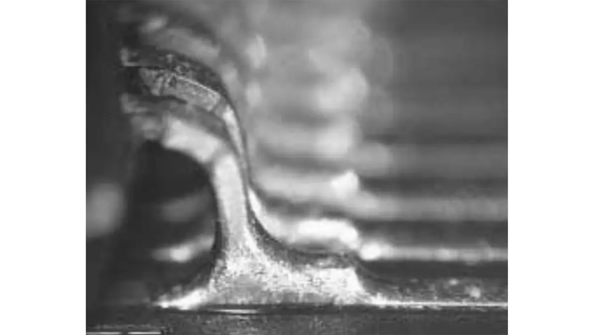
After metallographic analysis of the joint, it was shown that:

  • As the gold from the component lead is minimum, it is dissolved on the solder.
  • While the Sn melts during reflow, the sacrificial Au/Pd layer of the Surface is dissolved. The solder joint is made to the Ni surface of the component lead.
  • There is no Cu migration through the Ni barrier layer of the lead.
  • In a system with no Au on the PWB and with a standard Au thickness on the lead, there is not Au detectable in the bulk of the solder joint.
  • The Au from the PWB can migrate across the solder joint and appear at the lead/solder interface in the case of the NiPd-finished lead (no gold, previous finish used by Texas Instruments).
  • At very high Au thicknesses on PWB and leads but give Au concentrations of less than 3 weight %, acicular SnAu intermetallics do form. These do not appear to be enough toaffect pull strength.
  • The risk of Au embrittlement caused by NiPdAu component lead finish is essentially negligible.
  • 3% weight Au on the solder is only achieved for artificially high thickness on Au layer on the PWB.
  • Good solderability with SnPb and Pb free solders.

In conclusion, as NiPdAu finish does not pose risk of embrittlement, there is no need of performing degolding on parts using this finish.

featured image source: Texas Instrument

Related

Source: DoEEEt Blog

Recent Posts

Over-Voltage Protection Clippers, Clampers, Snubbers, DC Restorers

13.10.2025
13

Silicon Capacitors Market: Shaping the Foundation for Next-Gen Miniaturization Electronics

10.10.2025
32

Enhancing Energy Density in Nanocomposite Dielectric Capacitors

9.10.2025
28

Advances in the Environmental Performance of Polymer Capacitors

8.10.2025
61

Vishay Releases DLA Tantalum Polymer Capacitors for Military and Aerospace

8.10.2025
24

Benefits of Tantalum Powder Stress–Strain Curve Evaluation vs Conventional Wet Test

3.10.2025
26

Electrolyte Selection and Performance in Supercapacitors

3.10.2025
36

Connector PCB Design Challenges

3.10.2025
38

Researchers Demonstrated High Energy Ceramic Capacitors Stable in Wide Temperature Range

2.10.2025
25

How to Manage Supercapacitors Leakage Current and Self Discharge 

1.10.2025
48

Upcoming Events

Oct 15
20:00 - 20:30 CEST

Planar Design & Simulation

Oct 17
12:00 - 14:00 EDT

External Visual Inspection per MIL-STD-883 TM 2009

Oct 20
October 20 - October 23

Digital WE Days 2025 – Virtual Conference

View Calendar

Popular Posts

  • Buck Converter Design and Calculation

    0 shares
    Share 0 Tweet 0
  • Boost Converter Design and Calculation

    0 shares
    Share 0 Tweet 0
  • Flyback Converter Design and Calculation

    0 shares
    Share 0 Tweet 0
  • LLC Resonant Converter Design and Calculation

    0 shares
    Share 0 Tweet 0
  • What is a Dielectric Constant and DF of Plastic Materials?

    4 shares
    Share 4 Tweet 0
  • Ripple Current and its Effects on the Performance of Capacitors

    3 shares
    Share 3 Tweet 0
  • SEPIC Converter Design and Calculation

    0 shares
    Share 0 Tweet 0
  • Dual Active Bridge (DAB) Topology Explained

    0 shares
    Share 0 Tweet 0
  • MLCC and Ceramic Capacitors

    0 shares
    Share 0 Tweet 0
  • Flying Capacitors Explained

    0 shares
    Share 0 Tweet 0

Newsletter Subscription


Passive Components Blog

© EPCI - Leading Passive Components Educational and Information Site

  • Home
  • Privacy Policy
  • EPCI Membership & Advertisement
  • About

No Result
View All Result
  • Home
  • Knowledge Blog
  • PCNS

© EPCI - Leading Passive Components Educational and Information Site

This website uses cookies. By continuing to use this website you are giving consent to cookies being used. Visit our Privacy and Cookie Policy.
Go to mobile version