Passive Components Blog
No Result
View All Result
  • Home
  • NewsFilter
    • All
    • Aerospace & Defence
    • Antenna
    • Applications
    • Automotive
    • Capacitors
    • Circuit Protection Devices
    • electro-mechanical news
    • Filters
    • Fuses
    • Inductors
    • Industrial
    • Integrated Passives
    • inter-connect news
    • Market & Supply Chain
    • Market Insights
    • Medical
    • Modelling and Simulation
    • New Materials & Supply
    • New Technologies
    • Non-linear Passives
    • Oscillators
    • Passive Sensors News
    • Resistors
    • RF & Microwave
    • Telecommunication
    • Weekly Digest

    Binder Hybrid Connector Simplifies One Cable Automation

    Tapped Inductor Buck Converter Fundamentals

    TAIYO YUDEN Releases Mini Metal Power Inductors

    Molecular Memristor Shows Record 145 kH Emergent Inductance

    Planar vs Conventional Transformer: When it Make Sense

    Researchers Propose Next‑Gen Compact Memory Using Ultra-thin Ferroelectric Capacitors

    Nichicon ADN Automotive Hybrid Aluminum Capacitors Now Available in EMEA

    Wk 19 Electronics Supply Chain Digest

    Electrocaloric Multilayer Capacitors: Towards Quiet, Solid‑State Cooling Around Room Temperature

    Trending Tags

    • Ripple Current
    • RF
    • Leakage Current
    • Tantalum vs Ceramic
    • Snubber
    • Low ESR
    • Feedthrough
    • Derating
    • Dielectric Constant
    • New Products
    • Market Reports
  • VideoFilter
    • All
    • Antenna videos
    • Capacitor videos
    • Circuit Protection Video
    • Filter videos
    • Fuse videos
    • Inductor videos
    • Inter-Connect Video
    • Non-linear passives videos
    • Oscillator videos
    • Passive sensors videos
    • Resistor videos

    Tapped Inductor Buck Converter Fundamentals

    Planar vs Conventional Transformer: When it Make Sense

    Modeling Fringing Field Losses in Inductors & Transformers

    Why Power Inductors Use a Ferrite Core With an Air Gap

    Transformer-Based Power-Line Harvester Magnetic Design

    Thermal Modeling of Magnetics

    Standard vs Planar LLC transformers Comparison for Battery Chargers

    How Modern Tools Model Magnetic Components for Power Electronics

    Advanced Loss Modeling for Planar Magnetics in the Frenetic Planar Tool

    Trending Tags

    • Capacitors explained
    • Inductors explained
    • Resistors explained
    • Filters explained
    • Application Video Guidelines
    • EMC
    • New Products
    • Ripple Current
    • Simulation
    • Tantalum vs Ceramic
  • Knowledge Blog
  • DossiersNew
  • Suppliers
    • Who is Who
  • PCNS
    • PCNS 2025
    • PCNS 2023
    • PCNS 2021
    • PCNS 2019
    • PCNS 2017
  • Events
No Result
View All Result
Passive Components Blog
No Result
View All Result

How to Determine Chip Temperature

3.1.2025
Reading Time: 7 mins read
A A

This article written by Dr.-Ing. Martin Schulz, Global Principal, Application Engineering, Littelfuse, provides insight into how to determine packaging chip temperature.

The most prominent factor for determining the service life of a power-electronic system is the temperature development at the passive or semiconductor components itself. For this reason, it is very important to determine the chip temperature as accurately as possible.

RelatedPosts

Littelfuse Expands High-Voltage TVS Diodes

Littelfuse Presents Ultra-Miniature Half-Pitch SMT DIP Switches

Littelfuse NANO2 415 SMD Fuse Wins 2025 Product of the Year

The determination of a power chip device’s temperature often is not a trivial task. This is partially because strictly speaking there is no such thing as “the chip temperature”. All specifications in data sheets and in calculations on service life refer to a mathematical construct of a virtual chip temperature or virtual junction temperature Tvj.

The so-called in-situ measurement is the method of choice to measure the chip temperature in the laboratory. Here, the chip to be measured is first heated to precisely defined temperatures using a calibrated heating plate. A small measuring current is then injected, and the resulting forward voltage is measured. There is a linear relationship between the forward voltage and the temperature of the chip, provided that a constant and precisely known current is flowing.

The current must be chosen small enough, so that it does not itself contribute to the heating of the measured passive or semiconductor component. At the same time, it but must be sufficiently large to generate a measurable voltage. Values around 1% of the nominal current of the semiconductor to be tested have proven to be reasonable.

In turn, the chip-temperature can be determined from the correlation, which is unique and reversible, if the previously used current is used and the voltage on the component is known. The result of this laboratory measurement is based on a constant chip temperature and, due to the external heating, there is a homogeneous temperature distribution in the chip. This special case, which does not reflect the conditions in the real application, provides “the chip temperature” or the “junction temperature” Tj.

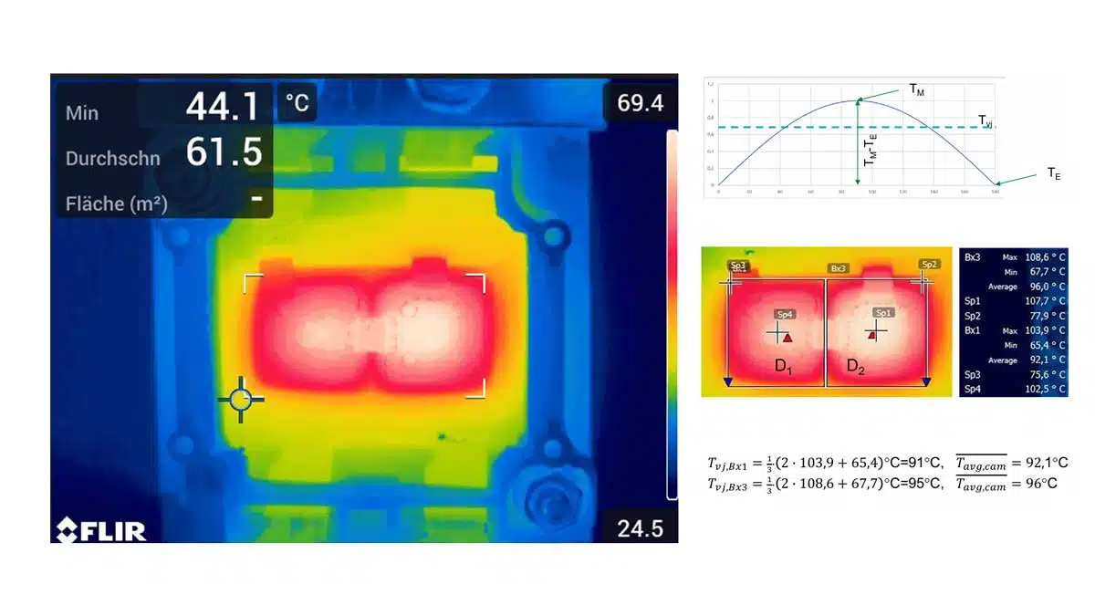
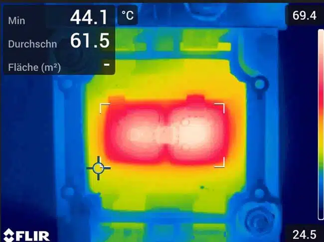
In the real application, however, there is a temperature gradient across the chip’s surface; the chip is hotter in the center than it is at the edges, especially at the corners. The reason for this is that more heat can be transferred to the surrounding assembly and connection technology at the edges and corners than in the center of the chip. The effect can be clearly seen in measurements such as those displayed in Figure 1, which are taken using an infrared imaging camera (IR).

Alternatively, a sensor placed on the chip is often used, for example a type K thermocouple. Although the sensor then provides a temperature value, this does not necessarily represent the value required for characterization and service life determination. One advantage of this measurement is that it is possible to measure during operation at high voltage and high current, provided the measurement equipment meets the requirements for the protection
of equipment and personnel. This is important as the sensor is in galvanic contact with the chip and therefore carries a potentially lethal voltage.

The temperature sensor is often placed in the center of the chip, so that it at least reliably delivers the maximum value. If the thermal relationships are known precisely enough, conclusions can also be drawn from the maximum value to the average value. The virtual chip temperature Tvj, which represents an average value of the temperature over the entire chip surface, is always of interest when considering the service life and thermal design. If it can be implemented, the in-situ measurement also precisely provides this value in the real setup, as only one voltage at one current needs to be measured. Averaging is an inherent part of this measurement setup. The measured voltage represents the chip temperature as if it were homogeneously distributed.

Reliability tests at component manufacturers are also monitored using the in-situ method. Here the approach is close to the application as the chip is actively heated. The information on load cycling resistance based on this method already includes the fact that the maximum temperature value on the chip is higher than the temperature specified. This approach can therefore be considered conservative and is ideally suited to characterization measurements and quality assurance processes.

Another way to calculate the mean value is by evaluating IR images. This method also allows the observation of semiconductors in real operation and provides precise and application-related information. For evaluation, the software belonging to the IR camera usually allows an area of interest to be defined and the correlating mean value within it to be determined. This procedure is used in Figure 1; the area under consideration comprises two diodes connected
in parallel. The disadvantage of this method is that the observed semiconductors must not be potted. Potting compounds, even if they are optically transparent, block the emitted infrared radiation, making this way of measurement impossible. Consequently, such setups cannot be operated with high voltages because the lack of insulation can lead to arcing and malfunction or even destruction.

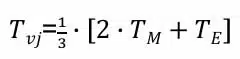
A frequently used alternative evaluation consists of determining the temperature TM in the center and the temperature TE in one corner of the chip and performing a 2-to-1 weighting. The virtual chip temperature then results in Tvj=1/3·(2·TM+TE). This is possible both from the IR image and using two correctly positioned temperature sensors. It is no coincidence that even this seemingly simple method delivers accurate values. The precision can be explained by the thermal conditions along the chip diagonals.

Figure 1: IR image of two diodes connected in parallel under DC load

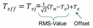
From one corner to the diagonally opposite corner, the temperature across the chip develops along a dome-shaped curve. A good approximation of this shape is either a parabola or a sinusoidal curve. Due to the simple relationships, the sinusoidal curve is the preferred one here. The mean temperature results from the effective value of the sine curve and the offset. Figure 2 depicts the curve that can be assumed in this case.

Figure 2: Temperature distribution along the diagonal of a chip

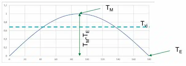
The required mean value corresponds to the RMS value, which is calculated from the amplitude (TM-TE) and the offset TE as:

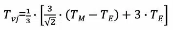
In another notation, the equation can be rewritten as:

with the approximation 3/SQRT(2) ~ 2 the result is:

A comparison of the three methods for averaging – in-situ, area average and 2/3 approximation – results in slightly different numerical values. If the tolerances of the respective measuring techniques are considered, it turns out that the values usually only deviate slightly from each other in the range of ±1K.

Figure 3: IR-evaluation of a thermal measurement

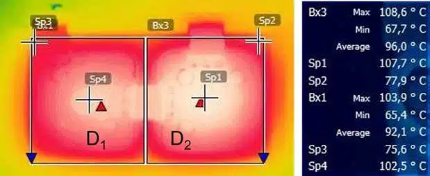
Figure 3 gives an insight into the data obtained using an IR camera from a measurement on two diodes connected in parallel within a semiconductor module.
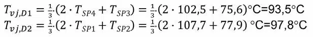
The measuring points Sp1 and Sp4 in the middle of the diodes and Sp2 and Sp3 at their corners, which are clearly visible in Figure 3, are used for the 1/2 weighting. These measuring points were placed by hand, so there are also tolerances here. Based on the local values determined, the virtual chip temperatures for the diodes are:

The evaluation of the mean value over the entered areas Bx1 and Bx3 and the automatically displayed maxima and minima provide:

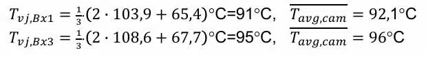
As a result, this means a temperature of 92.25±1.25°C for diode D1 and a temperature of 96.4±1.4°C for diode D2. Although in both cases neither the true maximum nor the true minimum was met, the deviation of values finally determined is negligible.

What is the practical use and gain for developers?

Determining the chip-temperature is crucial to support simulation results that are often starting points when predicting lifetime of a system under development. Chip temperature measurement during operation tends to be challenging. Thus, the recurring request is, to get a customized power device with a thermal sensor attached to the chip.

Instead – and if chip-sizes allow to do so – placing two sensors will get a very accurate result of the chip-temperature, even under operating conditions. The very similar results all methods lead to also substantiate how robust the 1/2 averaging is when there is a setup with two thermocouples.

Related

Source: Littelfuse

Recent Posts

Binder Hybrid Connector Simplifies One Cable Automation

13.5.2026
3

binder Releases Tool‑Tightenable M12 Connectors for Improved Reliability

30.4.2026
12

Kyocera Developed Multilayer Ceramic Core Substrate for AI Packages

30.4.2026
49

Heatsink Design and Thermal Interface Materials for Reliable Electronics

27.4.2026
35

Amphenol Explanded Liquid Cooling Connectors for AI, ESS and EV Systems

17.4.2026
32

Hirose Introduced BGA connector for PCIe Gen6 for AI and Edge Computing

17.4.2026
30

Molex Completes Acquisition of Smiths Interconnect, Expanding Portfolio of High-Reliability Connectivity Solutions

1.4.2026
19

Binder Introduces Triangular Moulding for M16 and M12 Cable Connectors

31.3.2026
14

Bourns Expands its Modular Contacts for Power-Dense Systems

19.3.2026
19

Upcoming Events

May 13
17:00 - 17:30 CEST

Winding Loss Modeling for Toroidal Magnetics – Including Gapped Cores

May 19
16:00 - 17:00 CEST

Designing Qi2 Wireless Power Systems: Practical Development and EMC Optimization

Jun 2
16:00 - 17:00 CEST

Calculation, Simulation and Measurement of 800V EMC Filters

View Calendar

Popular Posts

  • Buck Converter Design and Calculation

    0 shares
    Share 0 Tweet 0
  • Boost Converter Design and Calculation

    0 shares
    Share 0 Tweet 0
  • Flyback Converter Design and Calculation

    0 shares
    Share 0 Tweet 0
  • LLC Resonant Converter Design and Calculation

    0 shares
    Share 0 Tweet 0
  • MLCC and Ceramic Capacitors

    0 shares
    Share 0 Tweet 0
  • Dual Active Bridge (DAB) Topology

    0 shares
    Share 0 Tweet 0
  • What Electronics Engineer Needs to Know About Passive Low Pass Filters

    0 shares
    Share 0 Tweet 0
  • Capacitor Charging and Discharging

    0 shares
    Share 0 Tweet 0
  • Ripple Current and its Effects on the Performance of Capacitors

    3 shares
    Share 3 Tweet 0
  • MLCC Case Sizes Standards Explained

    0 shares
    Share 0 Tweet 0

Newsletter Subscription


Passive Components Blog

© EPCI - Leading Passive Components Educational and Information Site

  • Home
  • Privacy Policy
  • EPCI Membership & Advertisement
  • About

No Result
View All Result
  • Home
  • Knowledge Blog
  • PCNS

© EPCI - Leading Passive Components Educational and Information Site

This website uses cookies. By continuing to use this website you are giving consent to cookies being used. Visit our Privacy and Cookie Policy.
Go to mobile version