


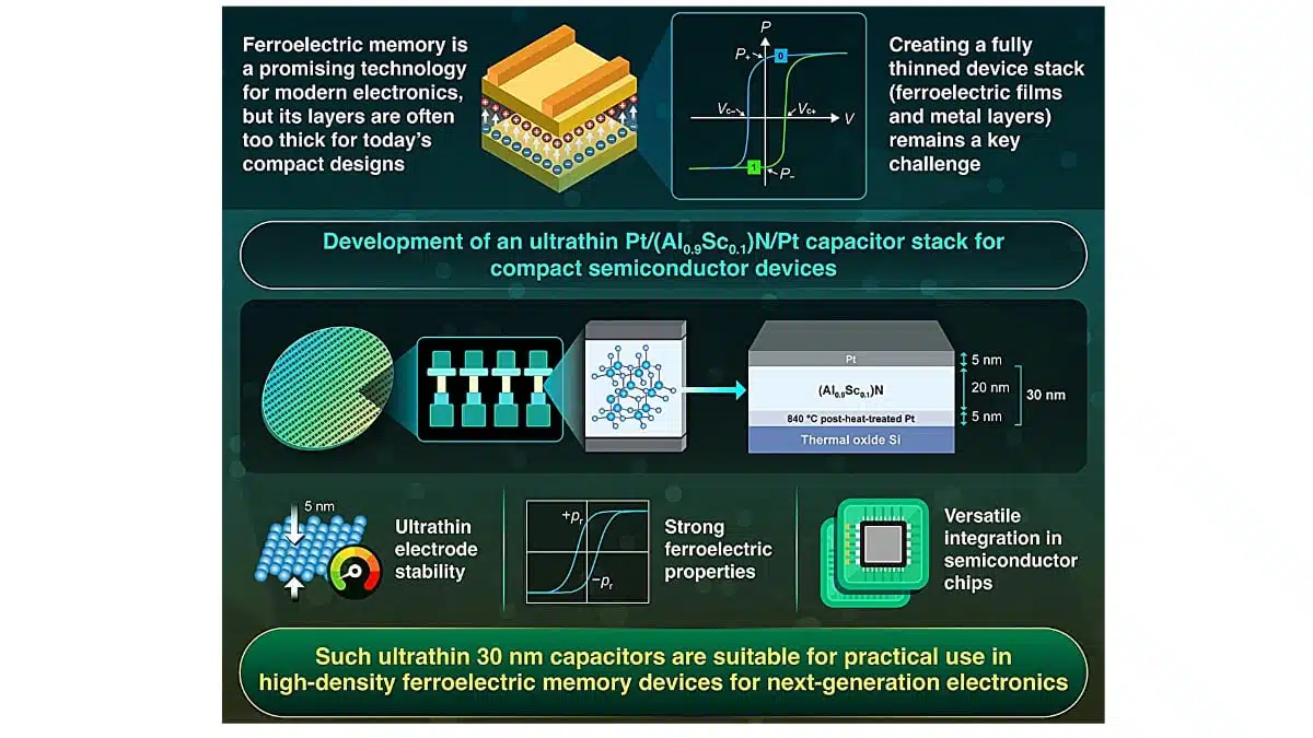
Researchers from Japanese research institutes investigated how to make ferroelectric memory components much thinner without losing performance.
Their work, published as an open‑access research article in Advanced Electronic Materials by Wiley, focuses on aluminum scandium nitride (AlScN) capacitors built with platinum electrodes and aimed at future low‑power, logic‑embedded memory chips. The study is supported by major Japanese funding agencies, including NEDO and JST, under programs targeting next‑generation integrated circuits and advanced materials.
Introduction
Modern computers still rely on separate chips for logic and memory, which wastes energy and time moving data back and forth. One promising solution is to place non‑volatile memory directly inside the logic chip, in the metal wiring layers, so‑called logic‑embedded memory. To make this practical, the memory cells must be extremely thin so that they fit between closely spaced interconnects without making fabrication too difficult.
Ferroelectric memories are attractive for this role because they can store data without power and can be switched with relatively low energy. Among ferroelectric materials, aluminum scandium nitride with a wurtzite crystal structure stands out thanks to its large switchable polarization and excellent stability at high temperatures and in hydrogen environments, both of which are important in semiconductor processing. However, in real devices the ferroelectric layer is always combined with metal electrodes on top and bottom, and until now very few studies looked at the total thickness of the complete capacitor stack, even though this total height is what limits integration.
In this work, the authors study a capacitor structure where an Al0.9Sc0.1N layer is sandwiched between platinum electrodes and show how far they can shrink every part of this stack. They systematically vary the thickness of the bottom electrode, the ferroelectric film, and the top electrode, analyze crystal quality with X‑ray diffraction and electron microscopy, and measure ferroelectric properties such as remanent polarization and fatigue. In the end, they demonstrate a complete Pt/AlScN/Pt stack only 30 nm thick that still offers very high remanent polarization, comparable to much thicker devices.
Key points
- The team realizes a Pt/(Al0.9Sc0.1)N/Pt ferroelectric capacitor stack with a total thickness of 30 nm: 5 nm Pt bottom electrode / 20 nm AlScN / 5 nm Pt top electrode.
- Even at this extreme scaling, the capacitors show saturated remanent polarization above 100 µC cm, a value typical of much thicker AlScN films.
- A continuous and well‑oriented Pt bottom electrode is essential: at 5–30 nm Pt the AlScN grows with good crystal orientation and high polarization, while at 1 nm Pt the electrode becomes discontinuous, the ferroelectric film loses orientation, and switching almost vanishes.
- High‑temperature post‑annealing of the 5 nm Pt bottom electrode (up to 840 °C) significantly improves Pt (111) texture and, in turn, the orientation and polarization of thin AlScN layers.
- With this optimized bottom electrode, 20 nm AlScN still shows saturated remanent polarization above 100 µC cm, and 10 nm films reach about 90 µC cm.
- X‑ray analysis shows that as AlScN thickness decreases, the in‑plane lattice constant shrinks, the out‑of‑plane constant grows, and a derived anisotropy parameter u decreases, indicating stronger crystal anisotropy and strain in thin films.
- Reducing the Pt top electrode from 100 nm down to 5 nm has little impact on ferroelectric hysteresis or remanent polarization for 20 nm AlScN.
- Fatigue tests reveal that thick stacks (80 nm AlScN with 100 nm Pt top) maintain polarization beyond 105 cycles, while 20 nm AlScN shows gradual degradation regardless of top electrode thickness, pointing to thickness‑ and interface‑driven fatigue mechanisms.
- The results provide practical guidelines for how thin AlScN and its electrodes can be made for logic‑embedded ferroelectric memories, and highlight the need for better‑matched or lower‑temperature bottom electrode solutions.
Extended summary
The core question in this study is how thin a real ferroelectric memory cell can be made when considering not only the active material but also its metal electrodes. For logic‑embedded memories placed in the back‑end interconnect stack of a CMOS chip, overall height is critical: if the memory pillar is too tall relative to its lateral dimensions, it becomes very hard to pattern reliably at advanced technology nodes. Competing technologies such as ReRAM and MRAM already target total stack thicknesses around 40–50 nm, so to be competitive a ferroelectric option needs to reach a similar or smaller thickness.
The authors focus on aluminum scandium nitride, specifically Al0.9Sc0.1N, which is a wurtzite‑type ferroelectric that can be grown by sputtering and shows large remanent polarization and good process robustness. They choose platinum as both top and bottom electrodes, because Pt tends to grow with a strong (111) texture, which supports c‑axis‑oriented growth of the wurtzite AlScN layer. The study is split into three main parts: scaling the Pt bottom electrode, scaling the AlScN layer on an optimized bottom electrode, and finally scaling the Pt top electrode.
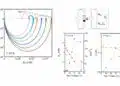
In the first part, the authors deposit Pt bottom electrodes between 1 and 30 nm thick on oxidized silicon, then grow relatively thick (160 nm) AlScN films on top to isolate the effect of the electrode thickness. X‑ray diffraction confirms that AlScN shows a (002) peak, indicating c‑axis orientation perpendicular to the substrate, and Pt shows a (111) peak for all electrode thicknesses. However, when they examine the rocking‑curve width, which measures how tightly the crystal orientations are aligned, they find that for 5–30 nm Pt the width stays around 2.0–2.3°, but for 1 nm Pt it jumps to about 7°. This means the 1 nm Pt films no longer provide a good crystallographic template for the ferroelectric layer.
Electrical tests support this structural picture. Using PUND measurements, the 160 nm AlScN films on 5–30 nm Pt show saturated remanent polarization well above 100 µC cm, whereas on 1 nm Pt the switching is almost absent. Transmission electron microscopy explains why: at 5 nm Pt, the electrode is continuous and the AlScN shows a uniform columnar structure, but at 1 nm Pt the metal breaks up into isolated grains and the AlScN above shows moiré patterns and misoriented growth. The authors conclude that a continuous bottom electrode of at least 5 nm is needed to keep both crystal orientation and ferroelectric performance at the desired level.
In the second part, they ask how far the AlScN thickness itself can be reduced if the 5 nm Pt bottom electrode is optimized. To do this, they subject the thin Pt electrode to a post‑heat treatment in vacuum between 450 and 840 °C. Rocking‑curve measurements of Pt (111) show that higher annealing temperatures, especially above 640 °C, sharpen the peak, indicating better orientation. Based on this, they choose 840 °C as the standard post‑anneal temperature for the next experiments. On these electrodes, they deposit AlScN films between 10 and 80 nm thick and, for comparison, grow an identical thickness series on non‑annealed Pt.
X‑ray diffraction patterns reveal that for all thicknesses the AlScN films remain c‑axis oriented: out‑of‑plane scans show only the (002) peak, and in‑plane scans show the (100) and (110) peaks typical of wurtzite structure with the c‑axis normal to the surface. From these data they extract the in‑plane lattice parameter a and the out‑of‑plane parameter , and compute an anisotropy parameter u defined by
As the AlScN thickness decreases, shrinks and expands, leading to a lower value of , which corresponds to stronger anisotropy and higher internal distortion of the wurtzite lattice. This effect is stronger when the Pt bottom electrode has been annealed, consistent with more coherent growth and increased in‑plane compressive strain due to the smaller Pt lattice constant.
At the same time, rocking‑curve widths of the AlScN (002) peak increase as film thickness decreases for both annealed and non‑annealed Pt, showing that orientation generally gets worse in very thin films, likely because of the relatively large lattice mismatch of around 12% between AlScN and Pt and the tendency of AlScN to align along its c‑axis. However, for 10 nm AlScN, post‑annealing the Pt clearly improves the rocking‑curve width, underlining that bottom‑electrode orientation and interface quality become increasingly critical as the ferroelectric layer gets thinner.
Ferroelectric measurements bring these structural trends into device‑relevant terms. On non‑annealed Pt, the AlScN films maintain saturated remanent polarization above 100 µC cm down to about 30 nm, but at 20 nm and below the polarization curves no longer saturate fully. On annealed Pt, by contrast, the authors obtain saturated remanent polarization above 100 µC cm even at 20 nm, and around 90 µC cm at 10 nm. Earlier work had suggested that lower values of the anisotropy parameter correlate with higher polarization, and here the combination of improved orientation and reduced in films on annealed Pt provides a consistent explanation. The drop in polarization at 10 nm is attributed to a mix of interfacial defects at the Pt/AlScN boundary, stronger strain effects in the ultrathin film, and increased disorder signaled by broader rocking curves.
In the final part of the study, the authors investigate the top electrode thickness. They fabricate capacitors with a fixed structure of 5 nm annealed Pt bottom electrode, 20 nm AlScN, and Pt top electrodes of 100, 15, or 5 nm. PUND measurements and polarization–electric‑field loops show that all these devices reach saturated remanent polarization above 100 µC cm and exhibit square hysteresis with clear switching currents. In other words, reducing the top Pt thickness from 100 nm down to 5 nm has only a small effect on ferroelectric behavior in this thickness range. This means the full stack can be reduced to 30 nm (5/20/5 nm) while keeping excellent ferroelectric properties.
The study also addresses endurance. The authors perform fatigue tests by repeatedly switching the capacitors and periodically checking the remanent polarization with PUND. For thicker devices with 80 nm AlScN and 100 nm top Pt, the polarization remains stable even after more than 10 cycles, comparable with previous results on similar ferroelectric systems. For 20 nm AlScN, however, the remanent polarization gradually decays from the early stages of cycling, and this degradation looks similar across all top‑electrode thicknesses tested. This suggests that the AlScN thickness and the bottom interface, rather than the top electrode, dominate fatigue behavior. The authors link this to thickness‑dependent lattice changes, orientation degradation, and potential interface damage at the Pt/AlScN boundary.
From an integration viewpoint, achieving a 30 nm total stack is a major step, as it places AlScN ferroelectric capacitors in the same vertical thickness range as ReRAM and MRAM cells designed for use in back‑end metallization layers. Nonetheless, the need for an 840 °C annealing step on the bottom Pt electrode poses a serious challenge for compatibility with standard CMOS back‑end processes, which usually have lower thermal budgets. The authors therefore point to the search for alternative electrode materials with better lattice matching to AlScN and lower‑temperature processing, as well as refined interface engineering, as key directions for enabling these ferroelectric stacks in real logic‑embedded memory products.
Conclusion
Doko and co‑authors show that it is possible to build a ferroelectric capacitor stack using Pt and Al0.9Sc0.1N with a total thickness of only 30 nm, while still delivering very high remanent polarization suitable for dense, low‑power, logic‑embedded memory applications. By carefully studying how bottom‑electrode continuity and orientation, ferroelectric film thickness, and lattice strain interact, they identify a practical lower limit of about 20 nm AlScN on a 5 nm Pt bottom electrode, and confirm that the top electrode can also be reduced to 5 nm without major performance loss.
The work also uncovers important limitations: ultrathin AlScN layers show reduced polarization and poorer fatigue, and the high‑temperature annealing required for Pt bottom electrodes conflicts with typical CMOS back‑end conditions. Looking ahead, the authors suggest that more suitable bottom‑electrode materials with better lattice matching and lower‑temperature processing, as well as improved interface control, will be necessary to turn these promising 30 nm AlScN ferroelectric stacks into manufacturable memory blocks on advanced logic chips.
References
- S. Doko, N. Matsui, T. Irisawa, K. Tsunekawa, N. Sun, Y. Nakamura, K. Okamoto, H. Funakubo, “Thickness Scaling of Integrated Pt/(Al0.9Sc0.1)N/Pt Capacitor Stacks to 30 nm,” Advanced Electronic Materials, 12(1), e00451, 2026, Wiley Online Library, open access under CC BY 4.0. https://doi.org/10.1002/aelm.202500451advanced.onlinelibrary.wiley