



Passive Components Blog
No Result
View All Result
  • Home
  • News
    • All
    • Aerospace & Defence
    • Antenna
    • Applications
    • Automotive
    • Capacitors
    • Circuit Protection Devices
    • electro-mechanical news
    • Filters
    • Fuses
    • Inductors
    • Industrial
    • Integrated Passives
    • inter-connect news
    • Market & Supply Chain
    • Market Insights
    • Medical
    • Modelling and Simulation
    • New Materials & Supply
    • New Technologies
    • Non-linear Passives
    • Optoelectronics and Isolation
    • Oscillators
    • Passive Sensors News
    • Resistors
    • RF & Microwave
    • Telecommunication
    • Weekly Digest
    Vishay Sfernice D2TO and DTO thick-film SMD power resistor sample kits with TO-263 D2PAK and TO-252 DPAK devices

    Vishay SMD Power Resistor Sample Kits for High-Power Design

    schurter-tcsv4-side-actuated-smt-tactile-switch

    SCHURTER Introduces Side-Actuated SMT Tactile Switch

    TLVR multiphase coupled inductors, auxiliary ballast inductor

    TLVR Coupled Inductors: Fast Load-Step Response and Current-Dependent Ballast-Inductor Optimisation

    Bourns CRH2512 2512 surface-mount metal-alloy current-sense resistor for high-current low-ohmic measurement

    Bourns CRH2512 5 W Current-Sense Resistors

    Littelfuse AK-FL FlatSuppressX axial-leaded bidirectional TVS diodes for high-voltage aviation DC power protection

    Littelfuse AK-FL TVS Diodes for Aviation DC Power Rails

    Rheinmetall Pierburg Pump Technology NanoLam DC-link capacitors for high-power electric vehicle traction inverter applications

    Rheinmetall Funds NanoLam Capacitor Production Scale-Up

    Bourns CSS4C-1216 four-terminal metal-strip current sense resistor for high-current Kelvin measurement

    Bourns Extends 1216 Kelvin Current Sense Resistors

    Modelithics COMPLETE+3D Library v26.3 for Ansys HFSS with RF passive component and 3D electromagnetic simulation models

    Modelithics COMPLETE+3D v26.3 Expands HFSS RF Models

    Samsung Electro-Mechanics low-profile and embedded MLCCs for compact PCB and power-delivery applications

    Samsung Low-Profile and Embedded MLCCs for Compact Devices

    Trending Tags

    • Ripple Current
    • RF
    • Leakage Current
    • Tantalum vs Ceramic
    • Snubber
    • Low ESR
    • Feedthrough
    • Derating
    • Dielectric Constant
    • New Products
    • Market Reports
  • Knowledge Blog
  • Dossiers
    • AI Hardware Dossier
    • Automotive Dossier
    • Industrial Robotics Dossier
    • Power Converter Dossier
    • Capacitor Dossier
    • Resistor Dossier
    • Inductor Dossier
    • Circuit Protection Dossier
  • Suppliers
    • Who is Who
  • PCNS
    • PCNS 2025
    • PCNS 2023
    • PCNS 2021
    • PCNS 2019
    • PCNS 2017
  • Events
  • Home
  • News
    • All
    • Aerospace & Defence
    • Antenna
    • Applications
    • Automotive
    • Capacitors
    • Circuit Protection Devices
    • electro-mechanical news
    • Filters
    • Fuses
    • Inductors
    • Industrial
    • Integrated Passives
    • inter-connect news
    • Market & Supply Chain
    • Market Insights
    • Medical
    • Modelling and Simulation
    • New Materials & Supply
    • New Technologies
    • Non-linear Passives
    • Optoelectronics and Isolation
    • Oscillators
    • Passive Sensors News
    • Resistors
    • RF & Microwave
    • Telecommunication
    • Weekly Digest
    Vishay Sfernice D2TO and DTO thick-film SMD power resistor sample kits with TO-263 D2PAK and TO-252 DPAK devices

    Vishay SMD Power Resistor Sample Kits for High-Power Design

    schurter-tcsv4-side-actuated-smt-tactile-switch

    SCHURTER Introduces Side-Actuated SMT Tactile Switch

    TLVR multiphase coupled inductors, auxiliary ballast inductor

    TLVR Coupled Inductors: Fast Load-Step Response and Current-Dependent Ballast-Inductor Optimisation

    Bourns CRH2512 2512 surface-mount metal-alloy current-sense resistor for high-current low-ohmic measurement

    Bourns CRH2512 5 W Current-Sense Resistors

    Littelfuse AK-FL FlatSuppressX axial-leaded bidirectional TVS diodes for high-voltage aviation DC power protection

    Littelfuse AK-FL TVS Diodes for Aviation DC Power Rails

    Rheinmetall Pierburg Pump Technology NanoLam DC-link capacitors for high-power electric vehicle traction inverter applications

    Rheinmetall Funds NanoLam Capacitor Production Scale-Up

    Bourns CSS4C-1216 four-terminal metal-strip current sense resistor for high-current Kelvin measurement

    Bourns Extends 1216 Kelvin Current Sense Resistors

    Modelithics COMPLETE+3D Library v26.3 for Ansys HFSS with RF passive component and 3D electromagnetic simulation models

    Modelithics COMPLETE+3D v26.3 Expands HFSS RF Models

    Samsung Electro-Mechanics low-profile and embedded MLCCs for compact PCB and power-delivery applications

    Samsung Low-Profile and Embedded MLCCs for Compact Devices

    Trending Tags

    • Ripple Current
    • RF
    • Leakage Current
    • Tantalum vs Ceramic
    • Snubber
    • Low ESR
    • Feedthrough
    • Derating
    • Dielectric Constant
    • New Products
    • Market Reports
  • Knowledge Blog
  • Dossiers
    • AI Hardware Dossier
    • Automotive Dossier
    • Industrial Robotics Dossier
    • Power Converter Dossier
    • Capacitor Dossier
    • Resistor Dossier
    • Inductor Dossier
    • Circuit Protection Dossier
  • Suppliers
    • Who is Who
  • PCNS
    • PCNS 2025
    • PCNS 2023
    • PCNS 2021
    • PCNS 2019
    • PCNS 2017
  • Events
No Result
View All Result
Passive Components Blog
No Result
View All Result

KYOCERA 10 µF 0201 MLCC Brings High‑Capacitance into Mobile Designs

6.5.2026
Reading Time: 8 mins read
A A

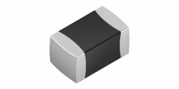
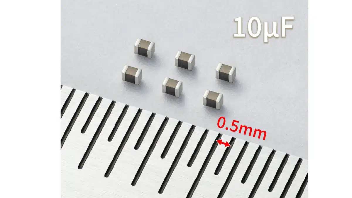
Kyocera has developed what it describes as the world’s first 10 µF multilayer ceramic chip capacitor (MLCC) in the EIA0201 size (0.6 × 0.3 mm), targeting space‑constrained smartphones and wearable devices.

The MLCC ceramic capacitor combines extremely thin dielectric layers with a high layer count to deliver large capacitance in a footprint where 10 µF was previously considered impractical, opening further options for decoupling and local energy storage close to advanced ICs.

RelatedPosts

KYOCERA AVX Adds 0201 C0G RF MLCCs to KGU Ultra-Low-ESR Capacitor Series

KYOCERA AVX Releases Vibration-Proof SMD Aluminum Electrolytic Capacitors for Harsh Industrial Designs

KYOCERA AVX Presents Antenna Integrator Studio Tutorial for Antenna Placement and RF Design

Key features and benefits

  • Ultra‑miniature footprint: EIA0201 size (0.6 × 0.3 mm) enables designers to increase total capacitance density or reduce PCB area in crowded RF and digital sections according to the manufacturer.
  • High capacitance class: 10 µF in this size class allows consolidation of multiple smaller capacitors into a single device, simplifying placement and potentially reducing mounting costs.
  • Advanced thin‑layer construction: Several hundred dielectric and internal electrode layers with thicknesses of 0.5 µm or less are used, supporting high capacitance in a very small volume while maintaining electrical performance according to Kyocera’s description.
  • Reliability‑driven process: Development focused on material technology (dielectric formulation, internal electrode composition) and process control (sheet forming, printing, lamination, firing) combined with detailed defect analysis, aiming to maintain quality despite aggressive miniaturization.
  • Support for future high‑stress applications: The technology platform is intended to extend toward higher temperature and higher electric‑field operation, which is relevant for automotive and semiconductor‑related equipment in later generations.

Example size and capacitance positioning

ParameterTypical value / note
Package sizeEIA0201 (0.6 mm × 0.3 mm)
Capacitance class10 µF in 0201 size
ConstructionSeveral hundred ceramic and internal electrode layers
Individual layer scaleDielectric layer thickness ≤ 0.5 µm according to Kyocera

Exact voltage rating, tolerance and temperature characteristics should be confirmed in the manufacturer’s datasheet once the commercial part numbers are published.

Typical applications

The initial focus for the 10 µF 0201 MLCC is in mobile and communication equipment, with a roadmap toward more demanding sectors:

  • Smartphones and tablet PCs, including application processors, RF transceivers and PMIC input/output decoupling.
  • Wearable devices such as smartwatches and fitness trackers, where extreme PCB density and height limitations make 0201 decoupling attractive.
  • Communications modules and IoT edge nodes requiring compact RF front ends and power management stages.
  • Future extensions into automotive electronics (for example, infotainment, ADAS domain controllers, connectivity modules) as higher temperature and reliability versions are introduced.
  • Semiconductor‑related systems and data‑center/AI server platforms once the ultra‑thin dielectric technology is adapted for higher field and temperature stress, according to Kyocera’s roadmap information.

In practice, a single 10 µF 0201 capacitor can be used very close to IC pins where only minimal land pattern area is available, complementing larger case‑size capacitors placed slightly further away in the power distribution network.

Technical highlights

The development of a 10 µF MLCC in EIA0201 required a combination of material science and process engineering improvements.

Thin‑layer dielectric and electrode technology

  • Kyocera reports stacking several hundred dielectric and internal electrode layers, each with a thickness on the order of 0.5 µm or less, to reach the targeted capacitance.
  • At these thicknesses, even a single conduction path between layers can cause a short circuit failure, so uniformity of ceramic layers, electrode printing and lamination becomes critical.
  • Achieving such thin layers typically involves optimized ceramic slurry formulation, precise tape casting or sheet forming, and high‑resolution internal electrode printing to avoid defects and edge overlaps.

Process and analysis flow

  • The company highlights the need to jointly develop material and process technologies: dielectric materials, sheet forming processes, internal electrode materials, printing conditions, lamination parameters and firing profiles are tuned together.
  • Analytical technologies such as short‑circuit failure analysis and microstructure evaluation are used to identify root causes of defects and feed lessons back into process standards.
  • According to Kyocera, repeated fundamental evaluations down to around 0.1 µm‑scale coatings were performed to establish internal standards and process windows designed to prevent defect occurrence rather than just screening out failures.

Cross‑functional project organization

  • The development team comprised engineers from three main departments: Development, Production Engineering and Manufacturing.
  • The Development department focused on new product design, creation of elemental technologies and analytical methods.
  • The Production Engineering department worked on new production methods and equipment start‑up, while the Manufacturing department concentrated on stabilizing mass production and quality.
  • This cross‑departmental approach is positioned as necessary to bring such an aggressive miniaturization project from concept to high‑volume production.

Design‑in notes for engineers

For practical design‑in of a 10 µF 0201 MLCC, engineers should consider both the opportunities and the constraints of operating at this miniaturization level.

  • Derating and operating conditions
    • Check the recommended DC voltage derating relative to the rated voltage (especially for X5R/X6S/X7R‑class dielectrics), since capacitance loss under bias can be significant in high‑k, ultra‑thin structures.
    • Review the specified operating temperature range and any guidance for high‑temperature use, particularly if evaluating future automotive‑grade versions.
  • Placement strategy in PDN
    • Use the 10 µF 0201 close to high‑pin‑count ICs where only tiny land patterns fit between balls or pins, complementing larger case sizes (0402/0603 and above) used for bulk decoupling.
    • Combine several units in parallel if layout allows, to reduce effective ESL and ESR and to improve transient response in high‑speed digital or RF SoCs.
  • PCB layout and assembly
    • Follow the manufacturer’s recommended land pattern and soldering profile to avoid mechanical and thermal stress on the extremely small body.
    • Pay attention to pad symmetry and stencil design to minimize tombstoning and skew during reflow, which become more critical at 0201 scale.
  • Reliability and quality considerations
    • As dielectric layers are very thin, adherence to the specified board flex, vibration and thermal cycling limits is important to prevent mechanical cracking.
    • For long‑life or safety‑critical systems (for example, automotive domains), confirm screening methods and reliability data, such as accelerated life testing, insulation resistance and failure modes, according to the manufacturer’s documentation.
  • Roadmap awareness
    • Kyocera indicates plans to extend this ultra‑thin layer technology to products capable of withstanding higher temperatures and electric fields, which may become relevant for next‑generation automotive and industrial platforms.
    • Early evaluation in consumer designs can help engineering teams gain experience with the technology before adopting future, higher‑stress versions in automotive or data‑center designs.

Example application positioning table

Use caseRole of 10 µF 0201 MLCC
Smartphone application processor core railLocal decoupling close to BGA pins in tight areas
Wearable PMIC outputSpace‑saving output smoothing in narrow layouts
RF transceiver supply railLocal energy storage with minimal loop area
Future automotive infotainment SoCHigh‑density decoupling around fine‑pitch packages

Source

This article is based on information from Kyocera’s official technical/project story describing the development of a 10 µF MLCC in EIA0201 size, complemented by related MLCC technical pages and catalog information provided by the manufacturer.

References

  1. Developer Interview – Behind the Development of Kyocera’s EIA0201 Model 10 µF Product MLCC
  2. Kyocera MLCC product overview
  3. Kyocera Capacitor Catalog (PDF)
  4. The Road to Thinner MLCCs and New Product Development
  5. Development of Highly Reliable MLCC – Evaluation and Analysis Technology Visualizes Areas of Deterioration


Related

Recent Posts

Rheinmetall Pierburg Pump Technology NanoLam DC-link capacitors for high-power electric vehicle traction inverter applications

Rheinmetall Funds NanoLam Capacitor Production Scale-Up

22.9.2026
44
Samsung Electro-Mechanics low-profile and embedded MLCCs for compact PCB and power-delivery applications

Samsung Low-Profile and Embedded MLCCs for Compact Devices

21.9.2026
24
Samsung Electro-Mechanics MLCC capacitor solutions for high-voltage converter snubbing and GPU power delivery

Samsung MLCC Options for 1 MW AI Rack Power

18.9.2026
31
Exxelia PM film capacitor and passive-component technologies for BepiColombo space electronics

Exxelia Passive Components Support BepiColombo Mission

16.9.2026
26
TDK B43657 and B43658 ultra-compact snap-in aluminum electrolytic capacitors for 500 V DC power-supply and DC-link applications

TDK Extends Compact Snap-In Capacitors to 500 V for AI Servers

16.9.2026
40

Samsung MLCC Revenue Seen Above KRW 8T by 2027, Murata EOL Actions Reshape Supply

11.9.2026
91

LG Innotek Demonstrates FC-BGA Substrates With Embedded Silicon Capacitors for AI Power Delivery

10.9.2026
75

Emerging Capacitor Markets in Fusion Energy

10.9.2026
68
onsemi solid-state transformer concept for 800 V HVDC AI data center power conversion with SiC modules, DC-link capacitors and high-frequency magnetics

Solid-State Transformers for 800 V AI Data Centers: Passive Component Design Considerations

9.9.2026
156

Upcoming Events

Sep 29
16:00 - 17:00 CEST

Cybersecurity 2026

Sep 30
15:00 - 16:00 CEST

Positronic Space and Military Connectors

Oct 14
17:00 - 18:00 CEST

Live Demo! Discover KYOCERA AVX Antenna Integrator Studio (AIS)

View Calendar

Popular Posts

  • Buck Converter Design and Calculation

    0 shares
    Share 0 Tweet 0
  • LLC Resonant Converter Design and Calculation

    0 shares
    Share 0 Tweet 0
  • Boost Converter Design and Calculation

    0 shares
    Share 0 Tweet 0
  • Flyback Converter Design and Calculation

    0 shares
    Share 0 Tweet 0
  • Capacitor Charging and Discharging

    0 shares
    Share 0 Tweet 0
  • Resistor Symbols

    0 shares
    Share 0 Tweet 0
  • Thermistors Basics, NTC and PTC Thermistors

    0 shares
    Share 0 Tweet 0
  • Audio Capacitors: Choosing Capacitors for Crossover Circuits

    0 shares
    Share 0 Tweet 0
  • Capacitor Symbols

    0 shares
    Share 0 Tweet 0
  • MLCC and Ceramic Capacitors

    0 shares
    Share 0 Tweet 0

Newsletter Subscription


Passive Components Blog

© 2015–2026
All rights reserved

  • Home
  • Privacy Policy
  • EPCI Membership & Advertisement
  • About

No Result
View All Result
  • Home
  • Knowledge Blog
  • Dossiers
  • PCNS

© 2015–2026
All rights reserved