Passive Components Blog
No Result
View All Result
  • Home
  • NewsFilter
    • All
    • Aerospace & Defence
    • Antenna
    • Applications
    • Automotive
    • Capacitors
    • Circuit Protection Devices
    • electro-mechanical news
    • Filters
    • Fuses
    • Inductors
    • Industrial
    • Integrated Passives
    • inter-connect news
    • Market & Supply Chain
    • Market Insights
    • Medical
    • Modelling and Simulation
    • New Materials & Supply
    • New Technologies
    • Non-linear Passives
    • Oscillators
    • Passive Sensors News
    • Resistors
    • RF & Microwave
    • Telecommunication
    • Weekly Digest

    Samsung Electro-Mechanics High Capacitance MLCCs for ADAS SoCs

    Murata Expands its Automotive Common Mode Choke Coils to 150C and High Current Capability

    Bourns Releases New Current Transformer

    Skeleton Releases GrapheneGPU to Reduce AI Energy Consumption by 44% and Boosts Power by 40%

    VINATech Expands Aluminum Capacitor Portfolio with Acquisition of Enesol

    binder Offers Wide Range of M12 Panel Mount Connectors

    Bourns Releases New Shielded Power Inductors for DDR5

    Supercapacitors Benefits in Industrial Valve Fail-Safe Control Systems

    Wk 21 Electronics Supply Chain Digest

    Trending Tags

    • Ripple Current
    • RF
    • Leakage Current
    • Tantalum vs Ceramic
    • Snubber
    • Low ESR
    • Feedthrough
    • Derating
    • Dielectric Constant
    • New Products
    • Market Reports
  • VideoFilter
    • All
    • Antenna videos
    • Capacitor videos
    • Circuit Protection Video
    • Filter videos
    • Fuse videos
    • Inductor videos
    • Inter-Connect Video
    • Non-linear passives videos
    • Oscillator videos
    • Passive sensors videos
    • Resistor videos

    Coupled Inductors Circuit Model and Examples of its Applications

    Inductor Resonances and its Impact to EMI

    Highly Reliable Flex Rigid PCBs, Würth Elektronik Webinar

    Causes of Oscillations in Flyback Converters

    How to design a 60W Flyback Transformer

    Modeling and Simulation of Leakage Inductance

    Power Inductor Considerations for AI High Power Computing – Vishay Video

    Coupled Inductors in Multiphase Boost Converters

    VPG Demonstrates Precision Resistor in Cryogenic Conditions

    Trending Tags

    • Capacitors explained
    • Inductors explained
    • Resistors explained
    • Filters explained
    • Application Video Guidelines
    • EMC
    • New Products
    • Ripple Current
    • Simulation
    • Tantalum vs Ceramic
  • Knowledge Blog
  • Suppliers
    • Who is Who
  • Events
No Result
View All Result
Passive Components Blog
No Result
View All Result

Smoltek’s New Zapping Method Accelerates CNF-MIM Capacitors Development

11.10.2024
Reading Time: 4 mins read
A A

Smoltek innovative “zapping” method drastically reduces development time and costs, enabling us to advance CNF-MIM silicon wafer based capacitor technology faster and making Smoltek Semi’s technology even more attractive to potential buyers.

While seeking buyers for our CNF-MIM technology, we continue to refine our offerings. Recently, we’ve made significant progress by tripling the capacitance density of our CNF-MIM capacitors while halving the leakage current with a new dielectric stack.

RelatedPosts

Smoltek is Closer to Establish CNF-MIM Capacitors Pilot Production

CNF-MIM Capacitors Benefits vs Deep Trench Capacitors

Smoltek Ready for Pilot Production of CNF-MIM Capacitors

To put this in perspective for non-experts, increased capacitance density means a greater ability to store energy in the form of electric charge within the same volume. Similarly, reduced leakage current means that the loss of stored energy is reduced, making our capacitors more efficient.

Such advancements boost the appeal of our technology to potential buyers. However, breakthroughs require extensive experimentation. To minimize time-to-market, we need rapid experiment setup capabilities. Manufacturing full CNF-MIM capacitors is time-consuming and costly. For quicker turnaround, we use parallel plate capacitors – simpler and cheaper to produce. Now, Smoltek Semi researchers have further accelerated and economized this process.

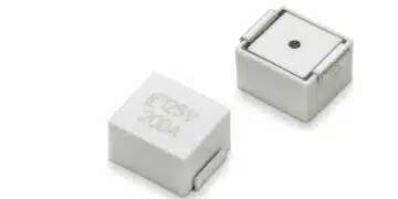
Parallel plate capacitors as proxies

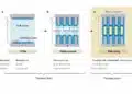
A parallel plate capacitor is the simplest form of capacitor: two metal plates separated by an insulator. CNF-MIM capacitors share this basic structure, but add carbon nanofibers to increase the metal surface area many times over. Both types consist of parallel metal surfaces separated by a dielectric stack of uniform thickness.

We manufacture parallel plate capacitors using the same methods and materials as CNF-MIM capacitors, including creating them on a silicon wafer substrate. The only difference is that we omit the carbon nanofiber steps for parallel plate capacitors. This similarity in production methods, minus the nanofibers, makes parallel plate capacitors excellent substitutes for testing CNF-MIM technology, as they mimic CNF-MIM capacitors while being simpler and quicker to produce.

Simplifying electrode access

Connecting an electrostatic capacitor requires access to both metal plates, each of which is called an electrode in this context. The top electrode is easily accessible, but the bottom electrode poses challenges. It’s covered by the top electrode and the dielectric stack, and can’t be accessed from below due to the substrate.

Previously, creating an electrical connection to the bottom electrode required several complex steps. Now, Smoltek Semi researchers use a method we call ”zapping” that significantly simplifies this process. While not a novel technique in itself, it’s new for us to apply it in this context. The zapping method involves applying a brief, high voltage across specific contact points on a test capacitor, creating a controlled breakdown in the insulating layer. This technique eliminates the need for multiple complex etching steps, significantly streamlining the testing process.

For those unfamiliar with electrical engineering, imagine trying to connect a wire to the bottom of a stack of sandwiches without disturbing the top layers. The old method was like carefully cutting through each layer to reach the bottom. The new zapping method is more like using a focused beam of energy to instantly melt a tiny, precise hole through the layers. This approach is much faster and causes minimal disruption to the overall structure, as it affects only a very small, controlled area.

It’s worth noting that zapping is a development tool that simplifies CNF-MIM capacitor characterization. It’s not intended for actual capacitor production.

Why zapping matters

Zapping reduces several fabrication steps for test capacitors, shortening iteration time from a month to a week. This acceleration allows more frequent testing of new configurations, speeding up research and optimization. It enables rapid evaluation of materials and design parameters, focusing efforts on critical components like the dielectric stack without lengthy production cycles.

Business impact

Zapping enhances Smoltek’s position by making development more cost-efficient and rapid. It reduces R&D expenses, allowing more experiments and technology refinement without overspending. This accelerated pace enables quicker delivery of preliminary results to potential partners, maintaining their engagement and interest.

In negotiations, demonstrating high-performing, cost-effective technology development makes Smoltek a more attractive partner. While zapping isn’t used in final production, the ability to iterate quickly ensures a reliable, scalable end product – key considerations for potential customers seeking easily integrated solutions.

Investor perspective

For shareholders, zapping translates into a clear advantage: faster development cycles mean a shorter time-to-market for breakthroughs, such as tripling the capacitance density and halving the leakage current, making CNF-MIM capacitors even more attractive to buyers.

Accelerating smart development

Zapping significantly reduces development time and costs, enabling faster iteration and maintaining our commercialization trajectory. It’s a pragmatic approach that bolsters our market position and enhances our appeal to potential buyers.

Related

Source: Smoltek

Recent Posts

Samsung Electro-Mechanics High Capacitance MLCCs for ADAS SoCs

30.5.2025
8

Skeleton Releases GrapheneGPU to Reduce AI Energy Consumption by 44% and Boosts Power by 40%

29.5.2025
27

VINATech Expands Aluminum Capacitor Portfolio with Acquisition of Enesol

28.5.2025
49

Supercapacitors Benefits in Industrial Valve Fail-Safe Control Systems

26.5.2025
28

Samsung Electro-Mechanics Releases High-Capacitance MLCCs for AI Server Applications

21.5.2025
54

Capacitor Ripple Current Testing: A Design Consideration

21.5.2025
67

Developing Low Inductance Film Capacitor using Bode 100 Analyzer

15.5.2025
49

YAGEO Extends Rectangular Aluminum Electrolytic Capacitor Family

15.5.2025
67

Dr. Tomas Zednicek Vision for Europe 2025 Passive Electronics Market

14.5.2025
61

Exxelia Power Film Capacitors Support Critical Systems Across Various Industries

13.5.2025
31

Upcoming Events

Jun 4
11:00 - 12:00 CEST

Würth Elektronik PCB Production in Asia

View Calendar

Popular Posts

  • Buck Converter Design and Calculation

    0 shares
    Share 0 Tweet 0
  • Boost Converter Design and Calculation

    0 shares
    Share 0 Tweet 0
  • SEPIC Converter Design and Calculation

    0 shares
    Share 0 Tweet 0
  • Flyback Converter Design and Calculation

    0 shares
    Share 0 Tweet 0
  • LLC Resonant Converter Design and Calculation

    0 shares
    Share 0 Tweet 0
  • Dual Active Bridge (DAB) Topology Explained

    0 shares
    Share 0 Tweet 0
  • Flying Capacitors Explained

    0 shares
    Share 0 Tweet 0
  • What is a Dielectric Constant and DF of Plastic Materials?

    4 shares
    Share 4 Tweet 0
  • Resistor Symbols

    0 shares
    Share 0 Tweet 0
  • Capacitor Symbols

    0 shares
    Share 0 Tweet 0

Newsletter Subscription


Passive Components Blog

© EPCI - Leading Passive Components Educational and Information Site

  • Home
  • Privacy Policy
  • EPCI Membership & Advertisement
  • About

No Result
View All Result
  • Home
  • Knowledge Blog
  • Premium Suppliers

© EPCI - Leading Passive Components Educational and Information Site

This website uses cookies. By continuing to use this website you are giving consent to cookies being used. Visit our Privacy and Cookie Policy.
Go to mobile version