


This article written by Dennis Zogbi, Paumanok Inc. published by TTI Market Eye provides an overview of 2025 resistor networks – its development, technology and configurations for thick/thin film resistor networks.
Thick Film Resistor Network Technology Overview
A traditional resistor network is composed of two or more resistive elements on the same insulating substrate.
Resistor networks are usually applied where there is a need for from four to 36 low-value resistors, because they save printed circuit board (PCB) real estate. In general, commercial networks have thick film elements and are available in either dual-in-line (DIP) packages which are traditionally molded plastic packages and the larger single-in-line packages (SIP) which are predominantly conformal coated designs produced in Asia.
We have followed the resistor network market for four decades because it combines two key raw materials in large quantities on a single component: the substrate that is used in resistor networks is predominantly 96% alumina, while the conductive interconnections are manufactured by screening precious metal powders in a volatile binder to form an ink or paste.
After the firing process, the composition forms a solid, low-resistance conductive pathway for the electrical current. A resistive ink formulation, which is predominantly made from a ruthenium cermet composition mixed with powdered glass frit and a volatile binder, is then screened over the ends of the conductors. The ink is then fired to form a hard resistive element.
Laser beams are then used to trim the resistance value to a precise level. Values of 10 ohms to 10 milliohms with tolerance ratings of +2 percent are the standard configurations. However, there are limitations to their design, predominantly in that each network can only handle less than 1/2 W, so the amount of dissipation each deposited resistor can handle is limited.
The end package is either plastic molded into a DIP or conformal coated into a SIP, as noted above. The variations to this market include the small thick film R/C network market (resistor + capacitor) and the specialty flatpack markets, which are variations on the thick film network market based upon either integration or number of resistors (a flat pack could have as many as 50 resistors per package).
Traditional SIP and DIP networks represent the oldest instance of the packaging of individual resistors to save time on pick and place costs and to maximize printed circuit board real estate. Industry leaders began packaging resistors into networks back in 1963. The SIP market is under constant threat of encroachment by the newer thick film multichip array, while the DIP market is threatened by encroachment by the newer thin film integrated passive devices.
Resistor chip arrays have been around for 30 years as a component configuration. Such devices offer a significant improvement in the “on-sertion” costs for PCB OEMs. In a chip array, 2, 3 or 4 chips (or even octels) are contained on a bridge. This enables these arrays to be placed on a board at the same time.
Summary Of Thick Film Resistor Network Products And Materials
Resistor Network, the Multichip Array Network
Resistor network array in surface mount configuration manufactured from ruthenium oxide resistive paste on a ceramic 96% alumina substrate in a quad or octel package. The array is a “pick and place” solution whereby customers save money on pick and place costs by picking and placing four or eight chips in an array at once. This product is consumed in many end markets where volumetric efficiency is a paramount design concern: portable computing, games and handsets.
Resistor Network, Coated SIP Network
Resistor network array manufactured from ruthenium oxide resistive paste on a ceramic 96% alumina substrate in a SIP – radial type unique lead. This unique configuration enables a complex solution for many individual components on the board while raising these parts off the board due to excess heat or moisture.
Resistor Network, SMD DIP Network
Resistor network array manufactured from ruthenium oxide resistive paste on a ceramic 96% alumina substrate in a dual-in-line package in a surface mount molded chip with gull type metal leads. Consumed in server computers and industrial motor controller as well as thermostat and telecom infrastructure applications.
Resistor Network, Molded DIP Network
Resistor network array manufactured from ruthenium oxide resistive paste on a ceramic 96% alumina substrate in a dual-in-line package – a surface mount package. Consumed in server computers, industrial motor controller and thermostat and telecom infrastructure applications.
Resistor Network, Molded SIP Network
Resistor network array manufactured from ruthenium oxide resistive paste on a ceramic 96% alumina substrate in a single-in-line molded package – a radial mount package. Consumed in computers and telecom infrastructure.
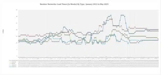
Resistor Networks Lead Time Trends By Type: January 2015 – May 2025
The legacy resistor network market is different from other passive component product markets we analyze. Some of these product lines can be scarce and it’s reflected in lead times, especially for the coated-SIP design. Other product markets reflect the steady state of the industry and the limited number of brand name vendors in the segment.
The May 2025 data supports this market for resistor networks as remaining somewhat stable for high-voltage applications in computing, industrial and infrastructure related components.
Ruthenium Supply Issues
Ruthenium is the key resistive element consumed by the global linear resistor industry in thick film network applications. Ruthenium is a rare earth metal that is mined primarily as a byproduct of other precious metal activities including platinum and palladium mining. Ruthenium metal is sourced primarily from South Africa processed into powders and then mixed with glass into paste for resistive inks.
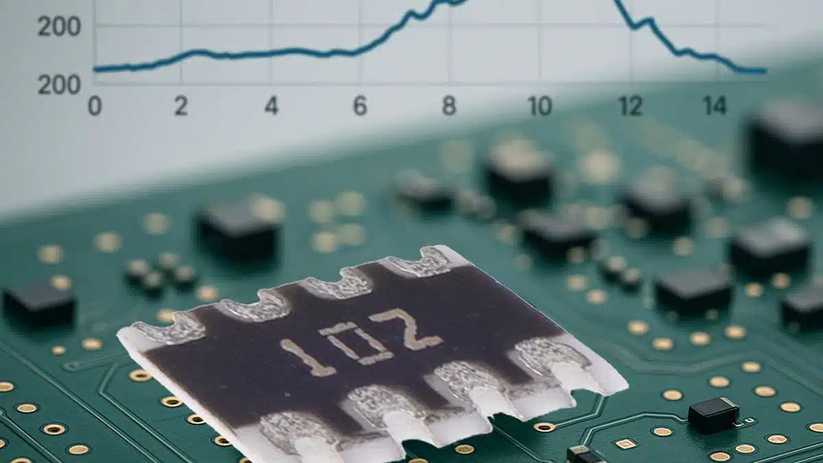
Ruthenium Price Trend per Troy Ounce by Month: April 2012 – May 2025 by Month
The ruthenium price has experienced significant volatility, and this has created excess demand for thin film alternatives based upon nickel. Ruthenium comes almost exclusively from South Africa and is a by-product of platinum mining.

Alumina Substrates
96% alumina substrates in the form of flat sheets and cylindrical cores are the primary substrate material consumed in thick film resistor networks. Alumina, or bauxite, is an abundant material used in the production of aluminum metal. There is no shortage of this material and nor do we anticipate one any time in the near future. For chips and arrays, the alumina board is sold by U.S., German and Japanese vendors for consumption by resistor network manufacturers. The boards are large and can accommodate hundreds or thousands of chip resistors per board. The manufacturer uses advanced laser cutting tools to separate the resistor from the board after resistive inks and glass passivation is applied.
Aluminum (Alumina Substrates)
Aluminum is produced from bauxite, which in turn is processed into alumina and aluminum. Alumina is used as a substrate for resistor networks and other resistor products (chips, axial and radial).

Applications For Thick Film Resistor Networks
Resistor networks are used in applications where the proximity of many resistors in one location on the board is replaced by a network solution. In 2025, the driving force behind consumption remains volumetric efficiency.
EMI/RFI Filtering
Advances in IC digital technology has created a stringent demand on limiting EMI/RFI levels in electronic equipment. EMI/RFI low pass filters are required in personal computers, data terminals, test equipment and process controllers for high frequency suppression into and out of the equipment. Resistor networks and ferrite beads are used to limit EMI/RFI in advanced electronic equipment.
Controlling EMI/RFI Emissions
Several approaches are employed to control EMI/RFI emissions, including gasketing, armored cables, power supply decoupling and low pass filtering of signal lines. Resistor networks are typically employed as low-pass filters when the noise components to be rejected occur at frequencies higher than the signal frequency to be passed.
Termination Applications
Resistor networks are also used to eliminate transmission line effects such as signal reflections and ringing which influence high speed CMOS. Resistor networks are therefore typically employed at the address, data and control buses connected to the CPU. Transmission lines will require termination when the time it takes the signal to travel from one end of the line to the other (the propagation delay) amounts to 1/2 or more of the edge rate of the signal (signal rise time or fall time).
Thus, in addition to the CPU busses, clock inputs, write and read strobe lines, chip select or output enable lines of static RAMs, PROMs and PLDs also employ termination networks.
Pull-up, pull-down applications: Resistor networks may also be used for “wire-OR” pull-up, ECL output pull-down, power pull-down pull-up, TTL/MOS interfacing, coding and decoding and telemetry.
Operational amplifier gain control applications: Resistor networks are typically used for controlling the gain in an operational amplifier. Other applications include stable reference, stable voltage division, stable feedback loops and for analog to digital or digital to analog conversion.
Voltage Divider Applications
Voltage dividers are used to step down voltages for analog processing. The application needs precise resistors to ensure that errors are not added during the conversion process. Multi-meters and oscilloscopes use voltage dividers.
Reasons For Market Growth Of Resistor Networks, Arrays And Thin Film Integrated Passive Electronic Components: 2025-2030
Volumetric Efficiency
The integration of many functions onto one single network is attractive to large OEMs because of the increased volumetric efficiency on the printed circuit board, especially for small, handheld portable electronic devices.
With respect to volumetric efficiency, resistor networks afford the end-user a better choice over thick film discrete devices because of the integration of many functions on a single network.
Savings on Pick and Place Costs
The OEM and EMS interest in placing many chips or functions on a board in a given location at a single time is a factor driving growth in the entire passive components industry. It is also justification for the growth of multichip resistor arrays, which serve the same purpose.
Summary And Conclusion
Resistor networks are an important part of the linear resistor supply chain and are composed of thick and thin film component solutions manufactured from alumina substrates and ruthenium-based thick film inks and pastes. Raw material costs for both key feedstocks have demonstrated price volatility due to the limited nature of supply. Lead times for SIP and DIP resistor networks have shown volatility in the past, largely related to limited component capacity to produce and volatility of the precious and base metal supply chains.
Regardless, surface mount and through-hole resistor networks are consumed in many applications where many passive components are found in proximity on the printed circuit board. These include filtering, termination, pull up/pull-down circuits as well as operational gain and voltage dividers. The market drivers behind their continued success continue to be volumetric efficiency and savings in pick and place costs per component.