Passive Components Blog
No Result
View All Result
  • Home
  • NewsFilter
    • All
    • Aerospace & Defence
    • Antenna
    • Applications
    • Automotive
    • Capacitors
    • Circuit Protection Devices
    • electro-mechanical news
    • Filters
    • Fuses
    • Inductors
    • Industrial
    • Integrated Passives
    • inter-connect news
    • Market & Supply Chain
    • Market Insights
    • Medical
    • Modelling and Simulation
    • New Materials & Supply
    • New Technologies
    • Non-linear Passives
    • Oscillators
    • Passive Sensors News
    • Resistors
    • RF & Microwave
    • Telecommunication
    • Weekly Digest

    Bourns Extends Rotational Life Option for its Guitar Potentiometer

    Modeling and Simulation of Leakage Inductance

    Power Inductor Considerations for AI High Power Computing – Vishay Video

    TAIYO YUDEN Releases Compact SMD Power Inductors for Automotive Application

    Fischer Releases High Vibration Robust Ratchet Locking USB-C Connector System

    Littelfuse Unveils High-Use Tactile Switches with 2 Million Cycle Lifespan

    KYOCERA AVX Releases Compact High-Directivity Couplers

    Supercapacitors Emerge as a Promising Solution to AI-Induced Power Energy Spikes

    Wk 18 Electronics Supply Chain Digest

    Trending Tags

    • Ripple Current
    • RF
    • Leakage Current
    • Tantalum vs Ceramic
    • Snubber
    • Low ESR
    • Feedthrough
    • Derating
    • Dielectric Constant
    • New Products
    • Market Reports
  • VideoFilter
    • All
    • Antenna videos
    • Capacitor videos
    • Circuit Protection Video
    • Filter videos
    • Fuse videos
    • Inductor videos
    • Inter-Connect Video
    • Non-linear passives videos
    • Oscillator videos
    • Passive sensors videos
    • Resistor videos

    Modeling and Simulation of Leakage Inductance

    Power Inductor Considerations for AI High Power Computing – Vishay Video

    Coupled Inductors in Multiphase Boost Converters

    VPG Demonstrates Precision Resistor in Cryogenic Conditions

    Comparison Testing of Chip Resistor Technologies Under High Vibration

    EMC Challenges for High Speed Signal Immunity and Low EMI

    MOSFET Gate Drive Resistors Power Losses

    Modified Magnetic Reluctance Equivalent Circuit and its Implications

    Improving Common Mode Noise Reduction while Decreasing BOM

    Trending Tags

    • Capacitors explained
    • Inductors explained
    • Resistors explained
    • Filters explained
    • Application Video Guidelines
    • EMC
    • New Products
    • Ripple Current
    • Simulation
    • Tantalum vs Ceramic
  • Knowledge Blog
  • Suppliers
    • Who is Who
  • Events
No Result
View All Result
Passive Components Blog
No Result
View All Result

Resistor Types, Construction and Features

4.3.2025
Reading Time: 11 mins read
A A

Resistor types can be divided into categories by various criteria.

The most common splits are by construction types, termination leads, used material or circuit function for applications.

RelatedPosts

Sulphur-Resistant Film Resistors

Designing with High Voltage Resistors: 10 Top Tips for Success

Overcoming the Challenges of Using Sub-Milliohm SMD Current Sense Chip Resistors

Thick film resistor technologies are the most often used, however what are the advantages, disadvantage compared to other thin film construction and MELF designs ?

Construction

  • fixed resistors
  • variable resistors (potentiometers, trimmers, rheostats)
  • non-linear resistors (thermistors, photoresistors. varistors, magnetoresistors, memristors)

Lead Types

  • Chassis Mount
  • SMD
  • MELF
  • Through Hole
  • Network

Materials

  • carbon film
  • carbon composite
  • ceramic
  • metal element
  • metal film and thin film
  • metal oxide film
  • metal foil
  • thick film
  • wire-wound

Applications – Circuit Function

  • current limiters
  • shunt measure
  • heaters
  • strain gauges

Major Fixed Resistor Technologies

Figure 1. Major fixed resistor technologies

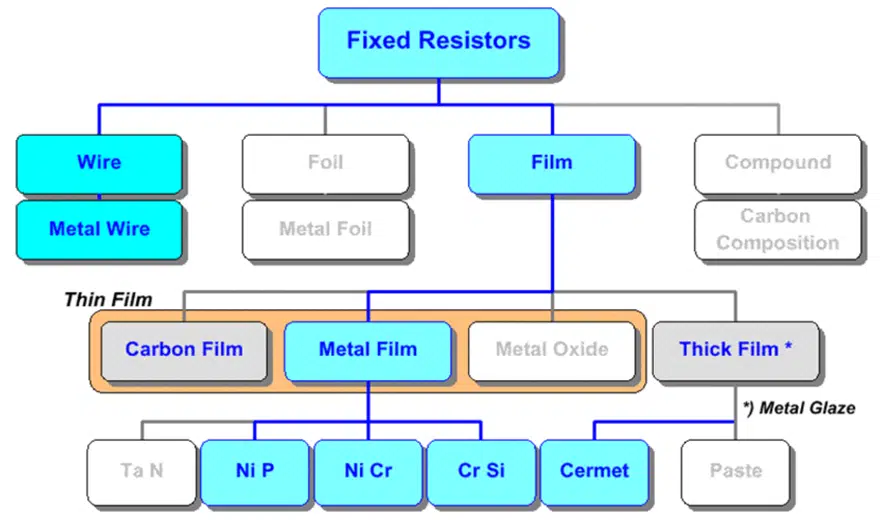
Thin vs Thick vs Foil and MELF Resistors Comparison

Comparing Thin Film vs. Thick Film Chip Resistors

Two of the most common chip resistor types in the market today are thick film and thin film technologies. Some characteristics of these two technologies are the same and some are quite different. Many of the performance differences of these two technologies are apparent from their specifications, but others are more subtle. This document will discuss the manufacturing processes and materials differences to explain how and why the two technologies perform as they do.

Figure 2. thick film chip resistor construction; source: Stackpole
Figure 3. thin film chip resistor construction; source: Stackpole

Thick Film

Thick Film Manufacturing Process
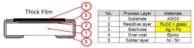
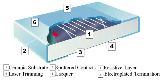
Thick film chip resistors are manufactured using a screen printing process like the process for screen printing t-shirts which many people are familiar with. The 96% alumina substrate is placed in the printing machine just below the screen and squeegee. The squeegee pushes the screen down to the substrate and pushes the material through the openings in the screen at the precise desired locations for the part design. As the squeegee moves across the substrate, the screen pulls itself away from the substrate leaving the material on the substrate. After each of these processes the material is dried and then fired at high temperature to sinter the thick film material to the substate and create a very robust and reliable electronic component.

The inner conductors, resistive element, dielectric, passivation and marking layers are all applied to a thick film resistor in this way. Prior to passivation, each part is tested and calibrated to its desired resistance value by means of a laser trimming process. Trimming raises the resistance value by removing some of the resistor element in a controlled way that lengthens the current path. Typically, all thick film resistors are manufactured to a resistance value slightly lower than the desired value, such that when they reach the calibration stage, it is easy to trim the parts up to their desired resistance value. This improves yield and helps to control manufacturing costs for this relatively inexpensive technology.

After trimming, a protective passivation layer is screen printed over the resistor element and parts that are 0603 size and larger are marked with their appropriate resistance value. The remaining processes provide the circuit connection through nickel barrier sputtering (vacuum deposition) to connect the top and bottom conductors and plating to provide the 100% matte tin termination for soldering.

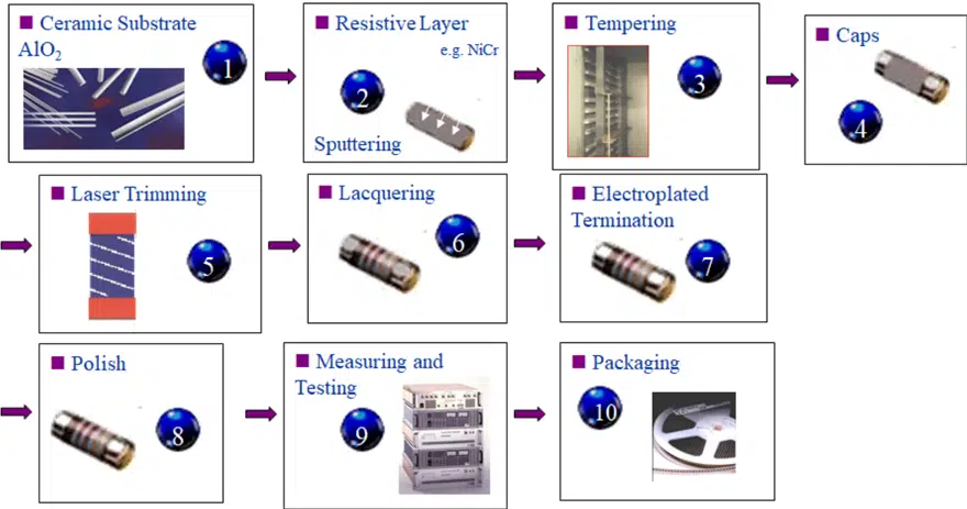
MELF Manufacturing Process

Figure 4. MELF resistors manufacturing process

Thin Film

Thin Film Manufacturing Process
Thin film chip resistor manufacturing (Figure 5. and 6.) typically starts with screen printing the inner conductors onto the ceramic substrate, drying and firing, like thick film chip resistors. From there the resistive elements are sputtered on in a chamber with very tightly controlled conditions and material targets. These targets contain the thin film metallic elements, in precisely controlled ratios, to produce the intended nominal resistance value. The sputtering process provides a very dense and uniform resistive element that is approximately a thousand times thinner than a comparable thick film element.

For certain resistance values with high precision requirements, photo etching may be used to precisely control the element dimensions and shape. The thin film elements are also calibrated using a laser to trim the element up in value to its desired resistance. The remaining processes are nearly identical to thick film in that the epoxy passivation and marking is applied to protect the resistive element, then the terminations are completed via nickel barrier sputtering to connect top and bottom and plating of 100% matte tin to provide the solderable connection for the PCB.

Figure 5. Thin film resistor construction – detailed
Figure 6. Thin film resistors manufacturing process

Thin Film vs Thick Film

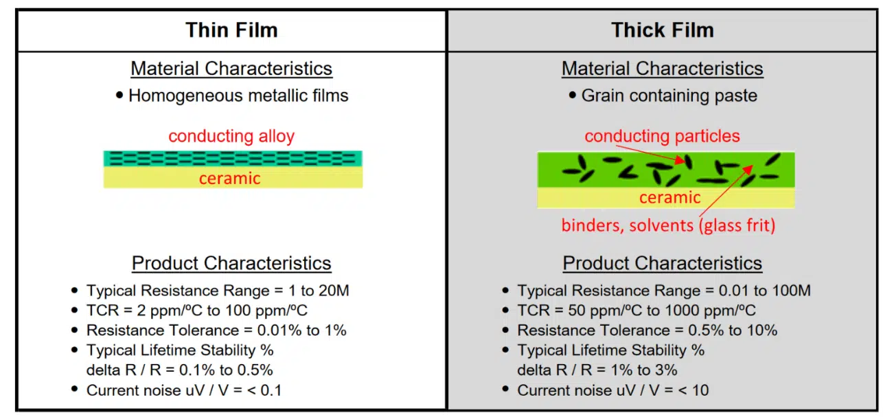
Thin film resistive elements have a high density homogeneous metallic alloy that is highly consistent and uniform. This makes the current path through the element very consistent, reliable, and repeatable. Thick film element materials are pastes containing metallic grains combined with glass frit binders, resins, and solvents. When fired, the element has a random nature to its conductive particles throughout the resistor element.

This randomness may lead to inconsistent current paths within the part and contributes to the electrical and environmental stability limitations that thick film technology has. However, the fired thick film element sinters itself to the ceramic substrate and becomes like glass, therefore the element has exceptional moisture stability. The most common thin film resistive elements are alloys containing nickel and chromium (Nichrome) which are susceptible to corrosion from high moisture environments. Only nichrome elements with special processing or tantalum nitride thin film elements resist moisture. See Figure 7.

Figure 7. Thin film vs. thick film resistors characteristics; source: Stackpole

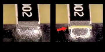
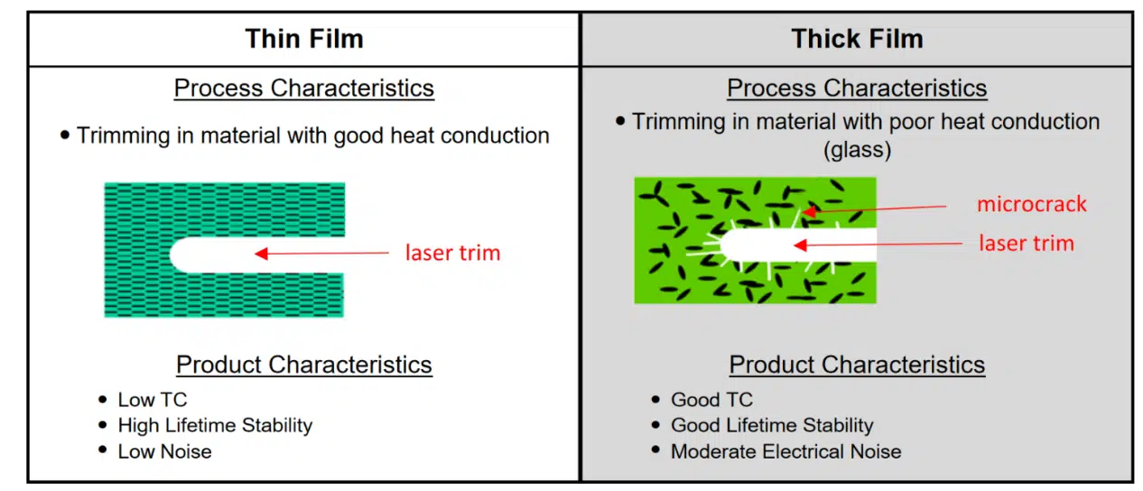
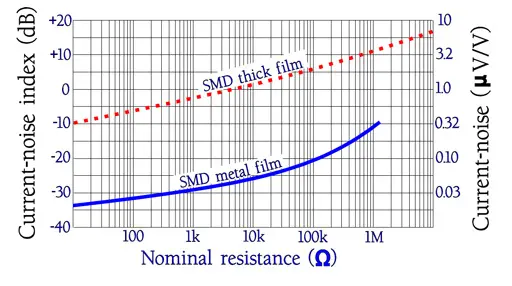
The trimming calibration process also creates substantial differences in thick film and thin film elements. Thin film resistors, being a metallic alloy with good heat conduction, will accept the laser trimming process with little effect on the material adjacent to the trim. Thick film elements, being glass-like, have poor heat conduction. Therefore, the material adjacent to the trim area will show microcracks where the material was heated as the laser passed through and subsequently cracked as it cooled. These microcracks lead to higher noise, poorer TCR, and higher resistance shift under typical environmental and electrical testing – Figure 8.

Figure 8. Thick film vs. thin film resistors trimming process characteristics; source: Stackpole

Main design differences of thin film vs thick films are shown on the chart below in Figure 9. comparing layer thickness vs achievable square resistance.

Figure 9. Thick vs thin film resistor technology domains

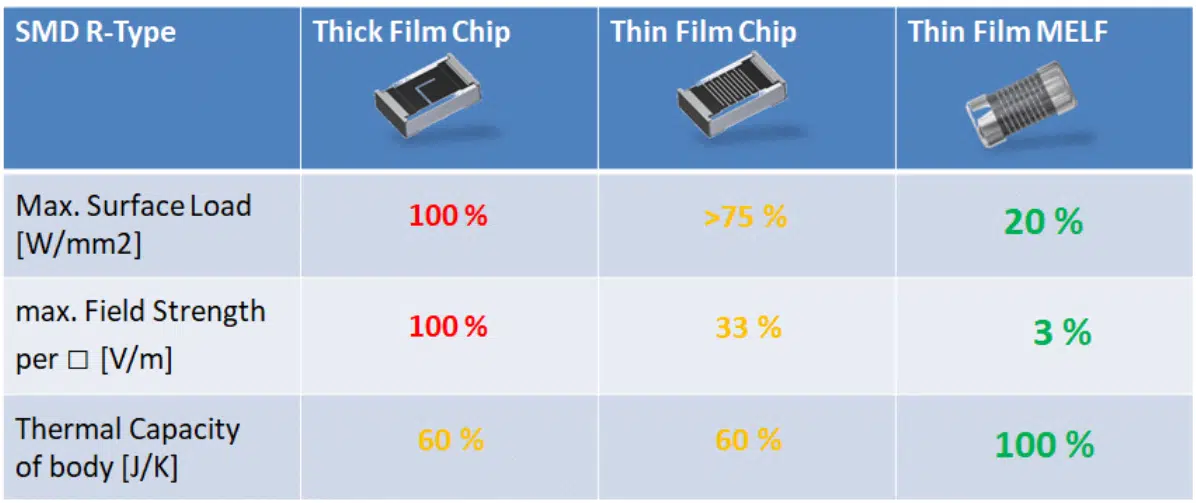
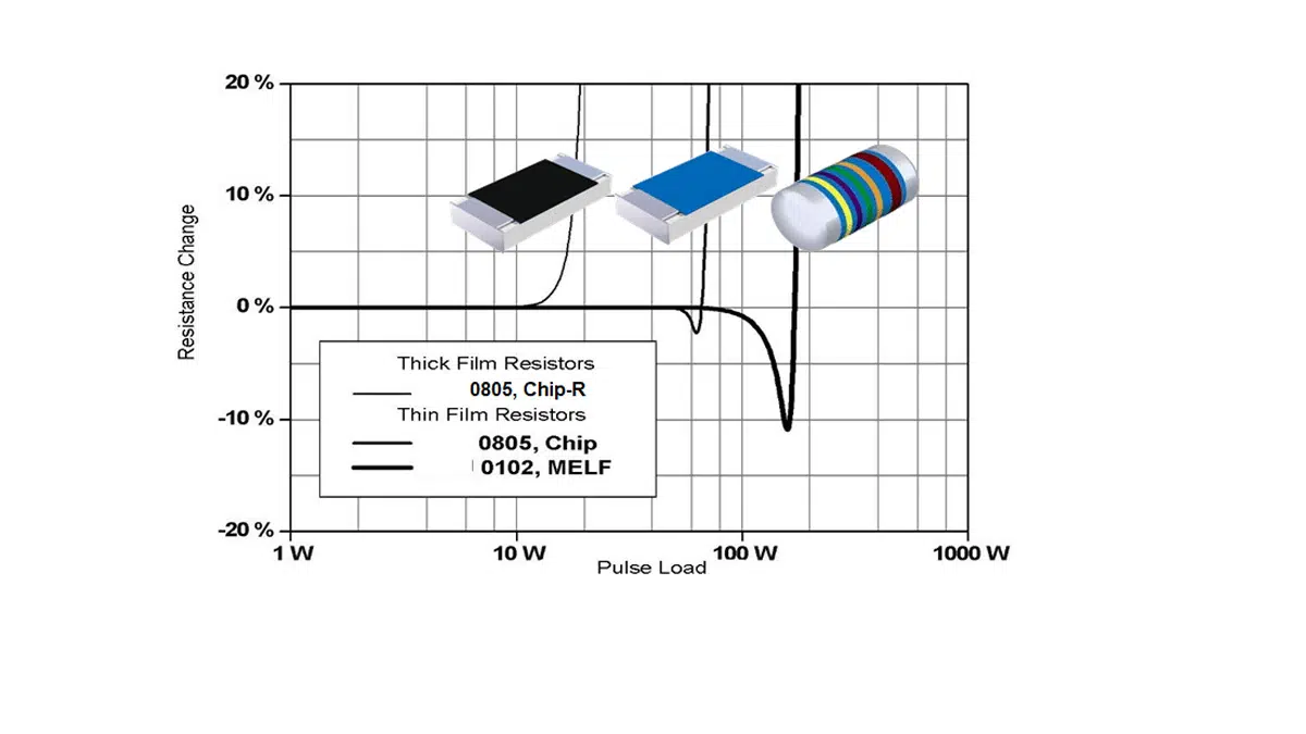
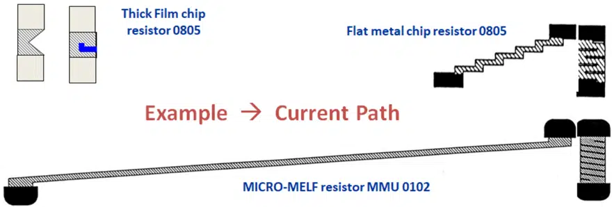
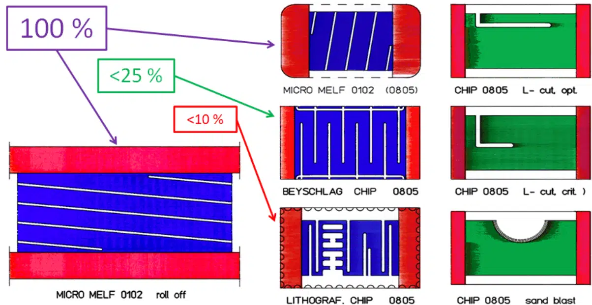
MELF capacitors that are also available in (micro)-chip case sizes have its advantage with possible path around the whole chip that makes it more efficient compare to Thick/Thin film SMDs. See the current path example on 0805 chip equivalent in Figure 10. below and pulse load capability comparison in Figure 11.:

Figure 10. Current path length example comparison on 0805 chip thick film vs thin metal chip film vs MELF resistors
Figure 11. Pulse Load capability comparison between thick film, thin film and MELF 0805 resistor designs

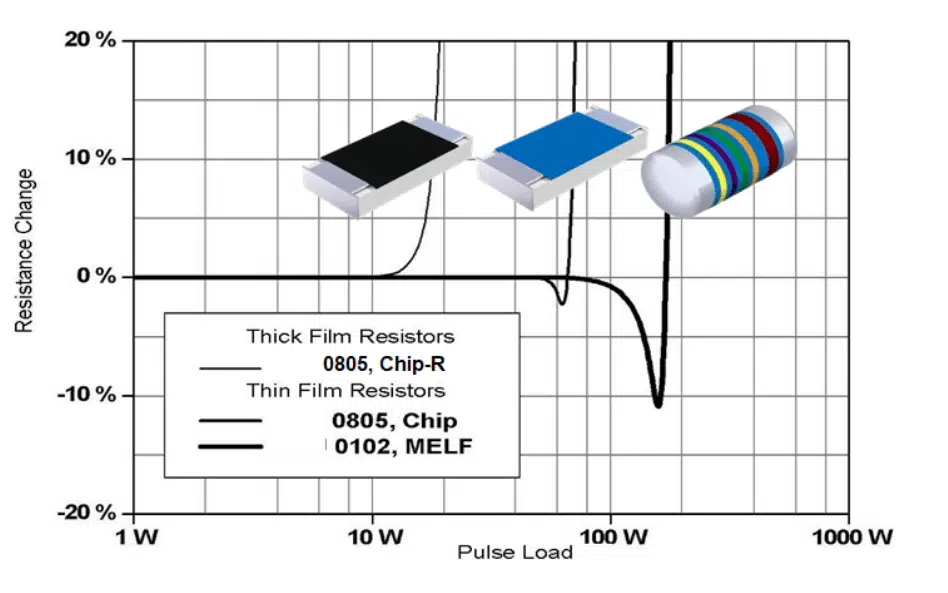
The differences in effective current length path are also reflected in the possible surface loads [W/mm2]. See the Figure 12. below.

Figure 12. Possible relative surface load comparison of MELF, thickfilm and thin film 0805 chip resistor; source: Vishay-Beyschlag

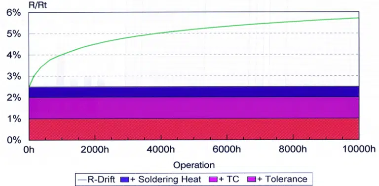
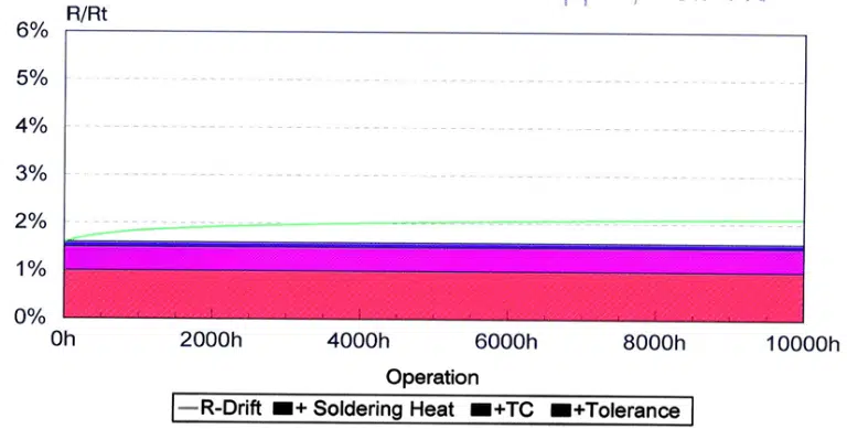
Thin Film vs Thick Film Resistors Stability

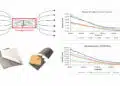
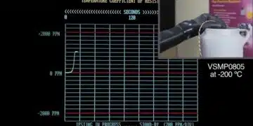
In general, thin film designs are providing better longer term stability, lower noise and robustness against soldering heat as shown in the following Figures 13.-15.:

Figure 13. Examples of typical resistor current noise versus resistance in two different resistor materials.

Thick Film

Figure 14. Stability of 1%-Thick film resistors, worst case tolerance and TCR

Thin Film

Figure 15. Stability of 1%-Thin film resistors, worst case tolerance and TCR

Thick vs Thin Film Summary Comparison


Thin film chip resistors offer the ability to achieve much better TCR and absolute resistance tolerances because of their material uniformity and consistency as well as their calibration process. The significantly higher element material density, the uniformity, and the improved heat conduction of the thin film element all provide better precision, stability, and lower electrical noise with improved high frequency characteristics.

The strength of thick film resistors is low cost, wider resistance range, and inherent moisture withstanding capability. Pulse handling for thin film is better for longer term pulses, but thick film resistors are better for short pulses of 0.0001 second and shorter.

Figure 16. Thick film vs Thin film vs Thin Film MELF resistors comparison
Figure 17. Thin film vs thick film resistors comparison; source: resistorguide.com

Related

Recent Posts

Modeling and Simulation of Leakage Inductance

9.5.2025
1

Murata and NIMS Built New Database of Dielectric Material Properties

5.5.2025
46

Shielding Cabinets

29.4.2025
17

Magnetic Shielding and Magnetic Shielding Sheets

29.4.2025
25

Corrosion its Development and Prevention

26.4.2025
25

Housing EMC Requirements, Issues and Solutions

26.4.2025
40

Hybrid Electrochemical Electrolytic Capacitor Provides High Frequency and High Capacitance Performance

25.4.2025
47

Non-Magnetic Interconnects

23.4.2025
13

RF Inductors Key Characteristics and Applications

17.4.2025
55

Electromagnetic Emissions Leakage in Enclosures

14.4.2025
40

Upcoming Events

May 14
11:00 - 12:00 CEST

Reliable RIGID.flex PCBs for Critical Applications – Made in Europe

May 14
17:00 - 17:30 CEST

Calculating Foil Winding Losses with AI

May 28
16:00 - 17:00 CEST

Power Over Data Line

View Calendar

Popular Posts

  • Buck Converter Design and Calculation

    0 shares
    Share 0 Tweet 0
  • Boost Converter Design and Calculation

    0 shares
    Share 0 Tweet 0
  • Tariffs Crush Sales Sentiment in April 2025 ECST Results

    0 shares
    Share 0 Tweet 0
  • Flyback Converter Design and Calculation

    0 shares
    Share 0 Tweet 0
  • What is a Dielectric Constant and DF of Plastic Materials?

    4 shares
    Share 4 Tweet 0
  • LLC Resonant Converter Design and Calculation

    0 shares
    Share 0 Tweet 0
  • Dual Active Bridge (DAB) Topology Explained

    0 shares
    Share 0 Tweet 0
  • Ripple Current and its Effects on the Performance of Capacitors

    3 shares
    Share 3 Tweet 0
  • SEPIC Converter Design and Calculation

    0 shares
    Share 0 Tweet 0
  • MLCC Case Sizes Standards Explained

    0 shares
    Share 0 Tweet 0

Newsletter Subscription


Passive Components Blog

© EPCI - Leading Passive Components Educational and Information Site

  • Home
  • Privacy Policy
  • EPCI Membership & Advertisement
  • About

No Result
View All Result
  • Home
  • Knowledge Blog
  • Premium Suppliers

© EPCI - Leading Passive Components Educational and Information Site

This website uses cookies. By continuing to use this website you are giving consent to cookies being used. Visit our Privacy and Cookie Policy.
Go to mobile version