DC-DC converters are fundamental building blocks used in electronics power management circuits. They convert one direct current (DC) voltage to another DC that is either a greater (step-up, boost) or lower (step-down, buck) voltage. Paul Golata, senior technology specialist at Mouser Electronics describes in his article published by TTI MarketEYE benefits of buck regulators as small, more efficient DC-DC converter designs.
Every part of an electronic design is like taking various building blocks and making them work together in harmony to accomplish the design goal. Electronic design engineers are always searching for further miniaturization of parts, increased functionality and higher reliability.
Today’s leading suppliers offer buck regulators with smaller footprints and as much as a one-third reduction in height, with significant improvements in power efficiency, transient performance, and electromagnetic interference (EMI).
MOSFETs (metal-oxide semiconductor field-effect transistors) are commonly employed as electronic switches. Buck regulators often utilize internal power FETs. As part of the effort to simplify buck regulators and reduce their size, especially for output currents of less than 20A, many parts are offered with a controller and integrated FETs within one package.
A controller with an integrated FET can compromise efficiency because, in specifying for a wide range of applications, these FETs’ voltage ratings can be much higher than those needed for a given application, resulting in increased switching losses. In addition, the dimensioning of the FETs will almost certainly be sub-optimal for a specific duty cycle – a significant compromise, especially in low-duty cycle applications.
Packaging technology is deployed to reduce the size and squeeze every possible milliohm of parasitic losses from the powertrain to glean efficiency improvements. Integration of complete powertrains—control plus FETs, output inductor, and input/output filters—is impeded primarily by the physically large inductors that are still required.
Updates to power architecture from leading suppliers resolve many of these issues, allowing for switching frequencies that remain in the 1MHz to 2MHz range while reducing the amount of inductance required – and also improving overall power conversion efficiency.
The current source used in this style of component is, in effect, an inductor in a buck stage – a close approximation to a current source, used to absorb all of the charge redistribution losses typically made in the switch. Because this current source inductor can be in the output stage, the energy, rather than being lost, can be recycled as useful energy to the load.
In this manner, the recycled energy allows the series resistance of the charge pump switch (and associated parasitic impedances) to be as small as possible due to the fact that inrush current is no longer an issue. This also minimizes the charge redistribution losses in this part of the circuit. In terms of efficiency, a charge pump with this design is 97 percent to 99 percent more efficient.
The charge pump itself is also two-phased and interleaved, and presents to the input an almost 100 percent duty cycle. When contrasted with a traditional buck regulator, where the duty cycle might be only 10 percent, this makes a massive difference to the input current ripple and the amount of input filtering needed.
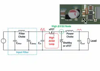
This approach to architecture also breaks down the whole voltage transition into many small voltage steps, executed across multiple input and output phases. Compared to single-stage buck designs, the net result is a much lower EMI signature for this architecture, for both conducted and radiated EMI. A major source of EMI in single-stage bucks is the inductor (V(t) = L * (di/dt)).
This type of DC/DC converter module is well-suited for use in PCIe/server applications, field-programmable gate array (FPGA), and digital signal processing (DSP), datacom/telecom systems, distributed bus architectures (DBA), programmable logic and mixed voltage systems. Select versions can also be used in I2C 6.0-compatible serial interfaces operating up to 1MHz.
This two-stage buck is an architectural innovation using standard off-the-shelf FETs in a very mature CMOS semiconductor process. Because the inductor is no longer the dominant component in the bill of materials, power conversion shrinks from occupying some 30 percent to 40 percent of a system’s circuit area to half of that, without compromising efficiency.
Furthermore, because the inductor usually is one of the tallest components in a system, this architecture allows for thinner solutions, improving packing density and enabling mobile devices to be slimmer.
Related article: How to Choose the Right Inductor for DC-DC Buck Applications


