


Consider now a structural definition of a connector. There are four basic components in a connector. They are:
A. the connector housing
B. the contact springs
C. the contact finish
D. the contact interface
This chapter will provide a basic introduction to connector housings, contact springs and contact finishes with details to be provided in following chapters. The contact interface will be discussed in detail in this chapter.
A few general comments are appropriate at this point. All connectors consist of two mating halves, a plug half which is inserted into the receptacle half. This plug/receptacle structure exists in both the housings and the contact springs. With respect to the contact springs, as mentioned earlier, in most connectors the plug contact deflects a spring system in the receptacle contact. This spring deflection produces the contact force which creates and maintains the desired metal-to-metal contact interface.
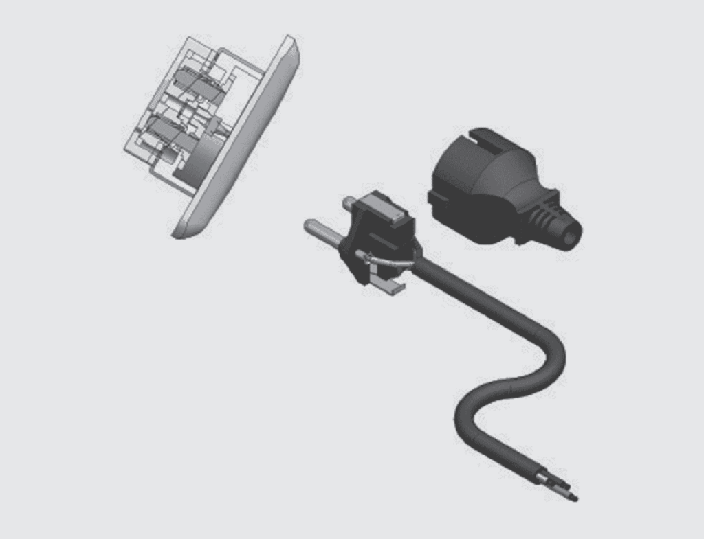
Consider these components as realized in a wall plug/receptacle connector as shown in Figure 1.2. The housing of the plug connector is overmolded onto the straight copper alloy plug contacts which are crimped onto the lamp cord wire. The housing of the receptacle connector is assembled around the copper alloy receptacle contacts which are pressure connected to the house wiring. When the connector halves are mated, the receptacle contact spring is deflected by the plug contact creating the contact interface. In this example, there is no contact finish, no plating or coating, on the contacts. The functions of a contact finish will be discussed in a following section.
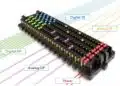
A cross section of a more typical connector is shown in Figure 1.2 with all components illustrated. Each of the connector components will be discussed briefly in this chapter and in detail in the following chapters.
Connector Housing
The connector housing, A in Figure 1.3, is the most obvious connector component and has four major functions:
Electrical insulation
All connectors have at least two contacts, input and output, which must be electrically insulated from each other. Most connectors have many more positions providing power or signals to the functional elements of the device. These multiple positions, too, must be electrically insulated from each other. Socket connectors for integrated circuit packages, for example, are available with more than a thousand positions. The insulation characteristics of a connector housing are dependent on both the design and material of the housing as will be discussed in Chapter II.
Dimensional stability
The two halves of the housing must mate together and, therefore, their mating features must be of corresponding shapes and on the same centerlines. The dimensional control required, obviously, depends on the size and the centerline spacing of the housing. Centerline spacings can vary from 0.3 mm (0.100 in) to 10 mm or even higher with corresponding decreases in dimensional tolerance requirements. The ability to realize these levels of dimensional control, both during molding of the housings and in field applications is an important consideration in housing design and material selection.
Mechanical support
In many connector designs the contacts are “latched” into the housing for mechanical support as well as dimensional control. Because spring deflections are responsible for creating the contact force, the mechanical stability of the support provided by the connector housing can have a significant impact on the spring characteristics of such connectors. Once again, this requirement impacts on the design and materials choices for the housing.
Environmental shielding
Most contact springs are made from copper alloys which are susceptible to corrosion reactions with oxygen, sulfur and chlorine, all of which are present in typical connector applications. Details of these processes will be provided in the second part of this chapter, Contact Finishes. At this point, it suffices to say that the design of the connector housing can have a significant impact on the environmental stability of a connector by shielding the contacts and contact interfaces from the environment.
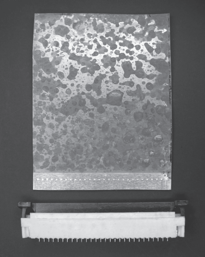
Figure 1.4 illustrates this shielding effect. The coupon shown is a copper plate. The coupon shown was exposed to a sulfur bearing environment while mated with the ZIF connector shown. Note the severe corrosion of the exposed portion of the coupon as compared to the shiny surface of the portion contained within the housing. Note also the wiping marks made by the receptacle contact springs as the coupon is inserted into the connector. This illustrates the cleaning effect that occurs during mating to wipe away surface films and contaminants.
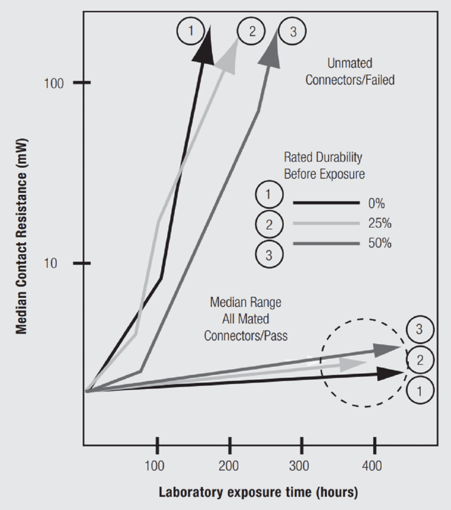
More important, however, is the data shown in Figure 1.5. This data will be discussed in detail in Chapter II/2.1 Contact Finishes. At this point it is sufficient to note that the data showing significant increases in contact resistance was from connectors which were exposed to the test environment unmated. That is, the plug and receptacle halves were exposed separately, while the stable resistance data was taken from mated connectors. The effectiveness of housing environmental shielding is clear. The shielding effect of connector housings provides an important contribution to the ability of connectors to remain functional in harsh environmental applications.
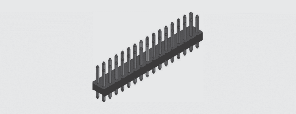
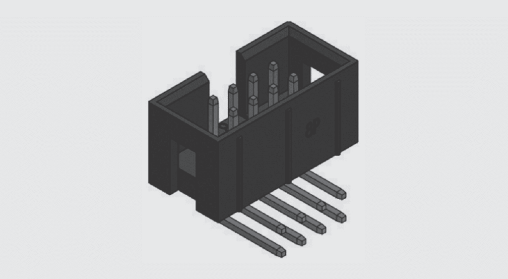
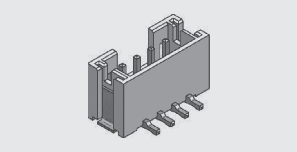
Connector housings vary in pin count from one to over a thousand, and in complexity from simple headers, Figure 1.6, to housings incorporating channels for air flow, Figure 1.7. Connector housing design, material selection and manufacturing practices will be reviewed in Chapter II/Design/Selection/Assembly.
Contact Springs
Electrical conductivity
The contact springs provide the electrical connection between the two sub-systems being connected. Copper alloys provide the highest electrical conductivity of commonly used metals when we consider the material price as well.
Separable Connections and Contact Force
As mentioned previously, the separable contact interface in a connector is created and maintained by the contact normal force generated by deflection of the receptacle contact springs by the plug contact on mating. For this reason, the contact normal force is arguably the most important connector design parameter as will be discussed in seperable connection chapter.
Plug contacts, Figure 1.8, include pads on a printed circuit board and rectangular or round pins, respectively. Receptacle contacts come in a variety of spring geometries to serve different application needs and requirements.
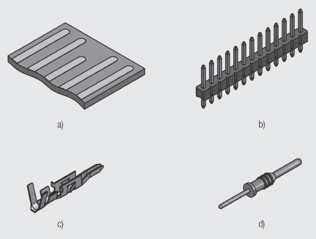
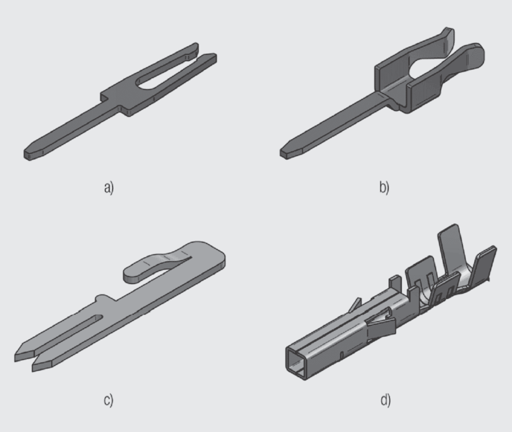
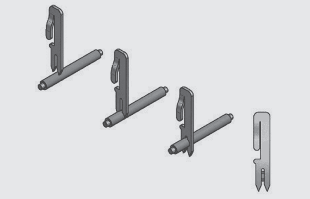
Figure 1.9 shows several receptacle spring geometries intended to provide functional capabilities, such as accommodating tolerances, and controlling the range of contact force in the connector. Copper alloys provide a good balance of spring characteristics and manufacturability. All of these contacts mate to a pin or post but require different amounts of forming to provide performance enhancements. Figure 1.9a is a simple flat stamping having twin cantilever beam contacts. The limitation of this contact is that the mating surfaces are the sheared edges of the stamping. This means a rough and uneven mating surface which is undesirable. If the contact was to be tin plated it could be used as is. But if silver or gold plating is desired the sheared edge would have to be improved eliminating the cost advantage. Figures 1.9b and 1.9c are simple means for eliminating the sheared edge issue. In Figure 1.9b the contact beams are simply twisted by 90 degrees so the mating surface becomes the rolled surface of the strip. The spring system is no longer a simple cantilever beam due to the twist which stiffens the beam. In Figure 1.9c the contact beams are folded upward to make the contact surface a rolled surface. The spring system is no longer a cantilever beam. The beam deflection will also open the U shape at the base of the beams. Finally, Figure 1.9d includes multiple forming operations to provide a crimped permanent connection with an insulation grip, latching beams to retain the contact in the housing and a box entry which provides an alignment feature as the pin or post is inserted into the contact.
Permanent connections
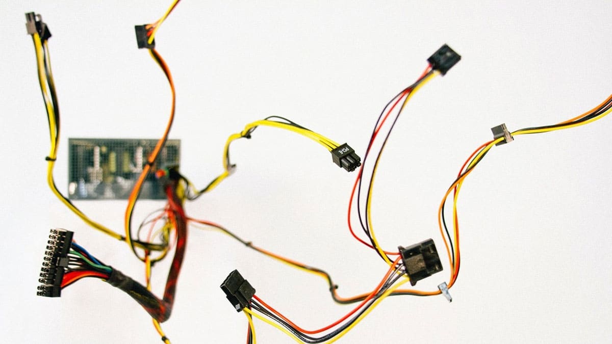
A connector also includes permanent connections between the connector contacts and the sub-systems being connected. Permanent connection methods used in connectors include both metallurgical and mechanical technologies. The primary metallurgical permanent connection method is soldering. There are two basic soldering technologies used in connectors, through hole and surface mount, examples of which are shown in Figures 1.10 and 1.11 respectively. The long solder tails in Figure 1.10 are inserted into plated through holes in a Printed Circuit Board (PCB) and wave soldered. The solder tails in Figure 1.11 are reflow soldered to surface pads on a pcb. Wave and reflow soldering will be reviewed in Chapter II/Design/Selection/Assembly. The two major mechanical permanent connection technologies are crimping and insulation displacement, examples of which are shown in Figures 1.12 and 1.13 respectively. Crimp and IDC technologies will be reviewed in Chapter II/Design/Selection/Assembly. Copper alloys are advantageous for both metallurgical and mechanical permanent connections because they are solderable/weldable and readily stamped and formed into the configurations needed to create mechanical permanent connections. Details of these technologies will be provided in Chapter II/2.2.2 Permanent Connections area. Details on copper alloy selection and manufacturing technologies as applied to connectors will be discussed in Chapter I/1.4 Connector Materials and Processes.
Contact Finishes
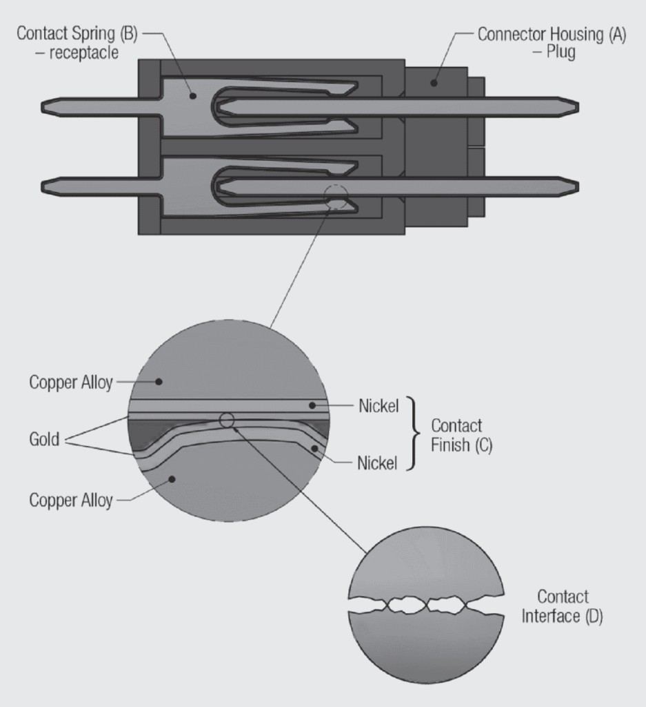
A contact finish, C in Figure 1.3, consists of a surface coating, generally produced by electroplating, over the contact spring to provide two performance benefits:
Corrosion protection for the contact springs and optimization of the electrical and mechanical characteristics of the contact interfaces. As mentioned, copper alloys are typically used as connector contact springs and are susceptible to corrosion in typical connector operating environments. The contact finish provides corrosion protection by covering the exposed copper to protect it from the operating environment. “Optimization” of contact interface performance is provided by influencing the corrosion and wear characteristics of the contact interface. These functions will be discussed in Chapter II.
There are two general types of contact finishes, noble and non-noble. Gold is the predominant noble metal finish material. The term “noble” refers to the fact that gold is not susceptible to corrosion. Tin is the most common non-noble finish material. Tin is susceptible to corrosion by the formation of a thin self limiting thickness of tin oxide. This oxide protects the contact interface from further corrosion, but is readily displaced on mating of the connector to provide the desired metal-to-metal contact interface.
A brief overview of each finish will be provided here with details to follow in Chapter II/2.1 Contact Finishes.
Noble Contact Finishes
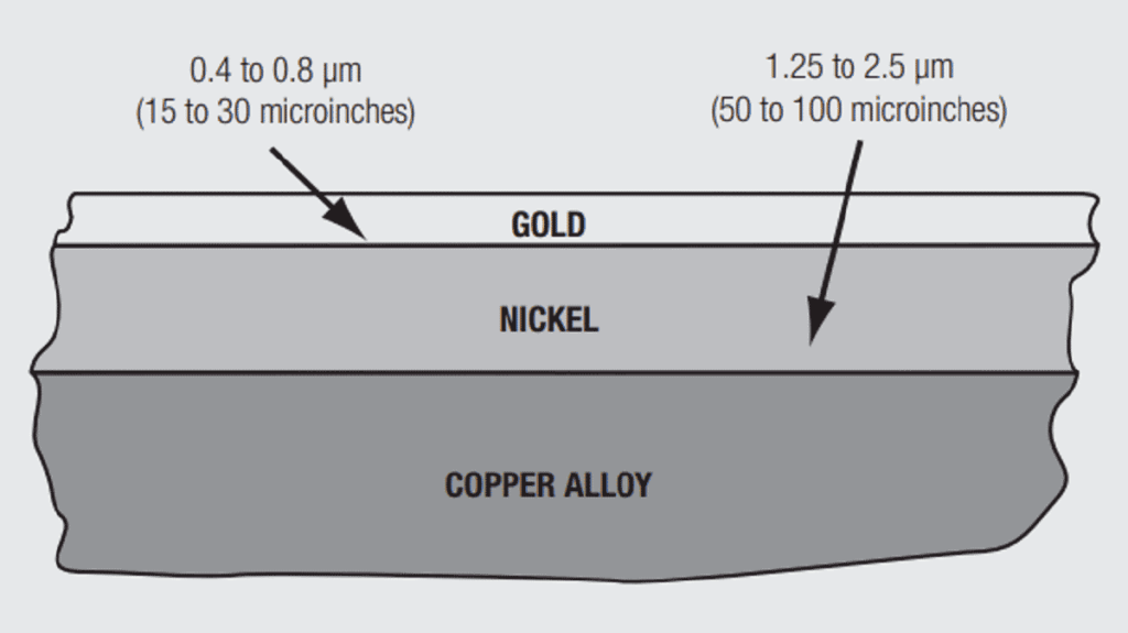
A noble metal finish is a system consisting of three components. A surface coating of noble metal, gold or palladium alloy, an underplate, generally nickel, and the base metal of the contact spring as shown in Figure 1.14. For Telecom or harsh environment gold and nickel are typically electroplated to thicknesses of the order of 0.4 to 0.8 µm (15 to 30 microinches) for gold and 1.25 to 2.50 µm (50 to 100 microinches) for nickel. Noble metal finishes are used in high performance and high reliability applications.
The gold top coat provides the corrosion protection. It also allows for performance optimization in that the hardness of the gold can be controlled to influence the friction and wear behavior of the mating interface. The nickel underplate provides several performance advantages noted here for reference with details to follow in Chapter II/ Design/Selection/Assembly.
The nickel underplate:
• reduces the susceptibility to pore corrosion
• reduces corrosion migration
• provides a diffusion barrier to base metal migration
• improves the mating durability of the contact interface
The contact spring is included in the noble metal finish system for both electrical and mechanical reasons. The electrical reason is that the distribution of the current flow to the contact interface is dependent on the conductivity of the contact spring. The mechanical reason is that the stresses applied to the contact interface during mating can extend down into the spring material due to the small thicknesses of the gold and nickel platings.
Non-noble Contact Finishes
The dominant non-noble finish is tin, with silver and nickel being used in selected applications. Tin is used in industrial and commercial applications including white goods, while nickel and silver are primarily used in battery contact and power contacts respectively.
These finishes are also typically electroplated, but tin can also be applied by dipping or reflow processes. Tin finish thicknesses are in the range of 2.5 to 5.0 µm (100 to 200 microinches). Nickel and silver thicknesses are generally in the range of 1.25 to 2.5 µm (50 to 100 microinches).