This article elaborates on design and calculation of basic DC/DC power converters. The post is based on Würth Elektronik‘s “DC/DC Converter Handbook” that can be ordered from WE website here. Published under permission from Würth Elektronik.
Key Takeaways
- DC-DC converters adjust voltage levels for electronic devices, playing a key role in applications like battery chargers and portable electronics.
- Common types include buck converters, which reduce voltage, and boost converters, which increase it.
- Design considerations for DC-DC converters include efficiency, stability, and EMC performance.
- Examples of widely used topologies are SEPIC and flyback converters, each serving specific needs based on input and output voltage requirements.
- Proper selection of inductors, capacitors, and input filters significantly affects converter performance.
DC-DC Power Converter Basic Characteristics
Every electronic device needs a power source with DC or AC voltage. While devices connected to the mains usually require the AC voltage to be rectified first, battery-powered devices already work directly with DC voltage.
Frequently, the available DC voltage does not match the powered circuit, so a DC/DC converter is needed to provide the required DC voltage and regulation. These DC/DC converters play a crucial role in various applications such as battery chargers, renewable energy and portable electronic devices where different voltage levels are required for proper operation.
DC/DC converters can basically be divided into two cases: A buck converter reduces a higher in put voltage to a lower output voltage, while a boost converter produces a higher output voltage from a lower input voltage. Example calculations can be found in Buck Converter Design and Calculation and Boost Converter Design and Calculation.
In addition, there are also DC/DC converter topologies that can operate with both higher and lower input voltages, so-called buck-boost converters. Typical representatives of this group are SEPIC converters and flyback converters. Example calculations can be found in SEPIC Converter Design and Calculation and
Flyback Converter Design and Calculation. It is important that a DC/DC converter operates as energy-efficiently as possible and at the same time provides a stable, regulated output voltage, even if the input voltage fluctuates or load changes occur on the output side. EMC behavior also deserves special attention. Thus, a DC/DC converter should be neither susceptible to interference nor interfere with other circuits in the environment.
In order to take these requirements into account, a designer of a DC/DC converter should first deal with selected basics. A good starting point is to deal intensively with rated and saturation currents when selecting the appropriate Selection of Storage Inductors for DC/DC Converters. The core material used in
the inductors has a major influence on the saturation behavior, the maximum possible switching frequency, and the component size. In the same way, the Selection of Capacitors for DC/DC Converters in terms of ripple current, impedance and the determination of the interference current is of great importance. Finally, the Input filters for DC/DC converters and the input stability criteria deserve attention.
Well prepared with the basic knowledge, one can then turn attention to the design examples of the following four widely used DC/DC converter topologies:
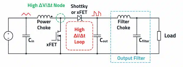
Among the switched-mode power supplies, the buck converter (step-down converter) is certainly the most widely used topology.
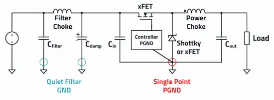
The buck converter is basically nothing more than a square wave generator with a downstream LC filter. It is obvious at first glance that, with regard to EMC, more attention must be paid to the input side than to the output side. From a functional perspective, “only” one capacitor is required at the input. This capacitor buffers the charge necessary for the current during the switch-on phase of the high-side FET and is recharged by the source during the switch-off phase.
If this converter is now placed at the input of the entire device electronics (e.g., Vin = 24 V) then further precautions must be taken regarding interference emission (EN 55032) and interference immunity (EN 55035). Even a suitably selected and well placed input capacitor is not sufficient to buffer the sometimes very high discontinuous currents over a wide frequency range.
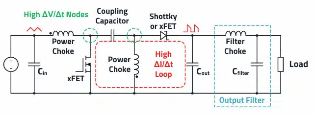
The boost converter (step-up converter) is used when the output voltage must be higher than the input voltage. The inductor is in the input circuit, which means that this topology has no discontinuous input current.
Because the storage inductor integrates the current over time, it has an almost triangular waveform, but this does not mean that the input side of the converter can be ignored in terms of EMC interference. The necessary input filters can therefore often be dimensioned slightly smaller than with the buck converter, for example. On the output side, a discontinuous, trapezoidal current flows in the boost converter.
It is apparent that the output side of the boost converter is more important from an EMC perspective than with the buck converter topology. The diode commutates hard on the output capacitor to which a discontinuous current is therefore superimposed. Depending on the application, the resulting RF
voltage as well as the low-frequency voltage ripple can interfere with the downstream electronics or is radiated as high-frequency interference. This means a downstream output filter may become necessary.
If the input voltage (e.g., lithium-ion battery) is larger or smaller than the output voltage during operation, then the SEPIC (Single Ended Primary Inductance Converter) topology is a possible choice.
This has the advantage of being inherently short-circuit proof thanks to the coupling capacitor in series with the MOSFET. A SEPIC converter can also be built with many common boost controller ICs, which offers advantages in terms of availability and cost. Another advantage of the SEPIC controller is that it does not draw discontinuous currents at the input and so does not unnecessarily load a battery.
Limitations do arise however with high output currents. As the most common SEPIC converters are built with Schottky diodes for commutation, this topology has lower efficiency at higher currents. Another critical component is the coupling capacitor. A very high AC current flows through this component from input to output. A capacitor with a very low ESR must therefore be used here; a parallel connection of several capacitors is also suitable for reducing the total ESR. MLCCs ceramic capacitors with X7R ceramic are ideally suited for this purpose.
Above 50 W, the fully synchronous buck-boost topologies are then usually beneficial due to the low RDS, on losses of the FETs used. However, with the fully synchronous buck-boost converters, the semiconductor cost ratio is relatively high, so that up to 50 W the SEPIC is often advantageous from a cost perspective.
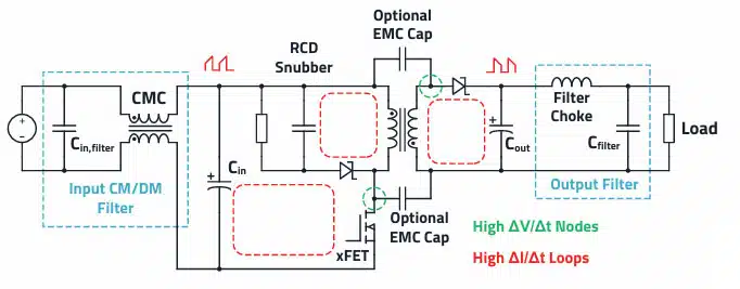
If one or more isolated, as well as regulated output voltages are needed, then the flyback converter up to approximately 150 W is often the best choice. This is mainly due to the fact, that it requires relatively few components, thus keeping the costs and space requirements low.
At higher power levels, other topologies, such as the forward converter, are advantageous because they also make better use of the transformer’s core volume. The flyback converter has trapezoidal discontinuous current curves at the input and output through the respective capacitors.
In practice, two EMC filters are therefore often necessary. As this converter has an isolated topology, common mode currents must also be increasingly expected above the switching frequency. This largely comes from the transformer’s parasitic coupling capacitance between the primary and secondary sides. Because of the high ΔV/Δt of the primary switching node (the hot node), a dielectric displacement current is superimposed on the secondary side via this coupling capacitance, which then flows via the ground (GND) to the primary side and during the EMC measurement of the interference voltage, via the LISN.
Common mode currents are also generated when an external MOSFET is used, and it is mounted on a heat sink or other metal surfaces. A parasitic capacitance arises between the MOSFET and the heat sink in this case, over which a dielectric displacement current also shows up. Many flyback applications
therefore use current compensated chokes in the input filter, as well as Y2 safety capacitors against ground. Capacitive current dividers can also be built from the primary to the secondary side with the help of the appropriate capacitors, which lead part of the common-mode currents back to the source by the shortest route. Should the application require reinforced insulation between input and output, Y1 capacitors must always be used for safety reasons. A downstream LC filter is often required to reduce the voltage ripple at the output. This filter also reduces interference up to approximately 30 MHz.
Beyond the ideal formulas below, it’s useful to see which passive components actually dominate the design effort for each of these topologies:
| Topology | Isolation | Typical power range | Dominant passive components | Primary passive concerns |
|---|---|---|---|---|
| Buck | No | <1 W – 10 kW | Storage inductor, output capacitors | Inductor saturation and loss; Cout ripple and impedance shape |
| Boost | No | <1 W – kW | Output capacitor, inductor, snubber network | High Cout RMS current; inductor thermal limits; EMI |
| SEPIC | No | <50 W | Coupling capacitor, coupled inductors, Cout | Coupling capacitor AC stress; core loss and leakage |
| Flyback / active clamp | Yes | <200 W | Transformer, clamp/snubber, Cout | Transformer loss; leakage energy; isolation; output ripple |
Source: Passive Components for Power Converters Dossier, Passive Components Blog (Table 3, Topologies and Their Dominant Passive Components).
A broader comparison across additional topologies (LLC resonant, dual active bridge, switched capacitor) can be found in the Power Converter Dossier.
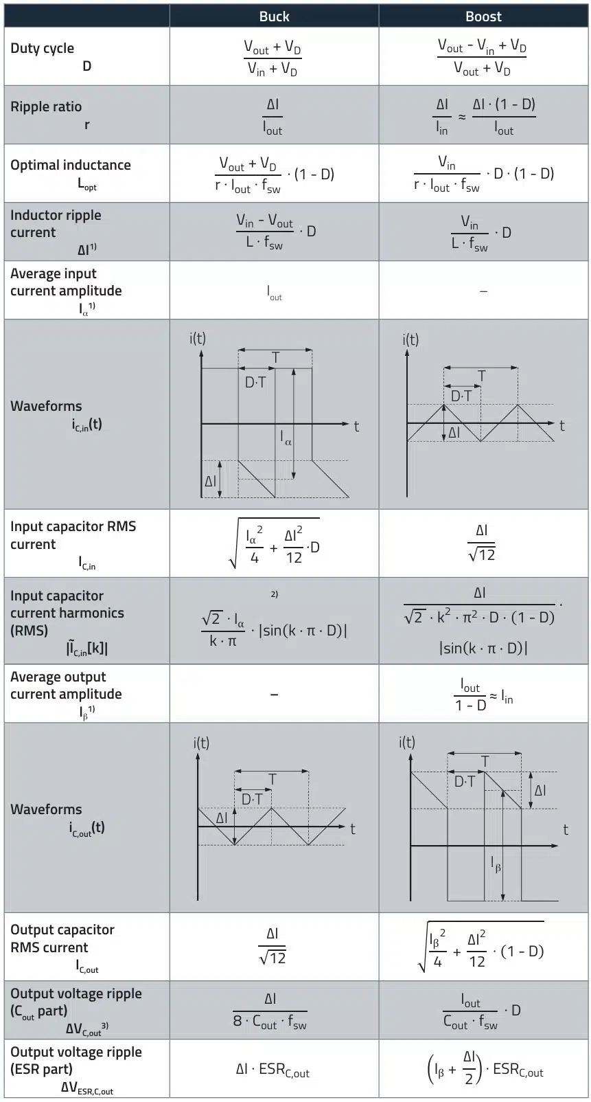
Buck and Boost Converter Basic Formulas
The following table 1. provides basic formulas of the buck and boost converter topologies.
SEPIC and Flyback Converter Basic Formulas
The following table 2. provides basic formulas of the SEPIC and flyback converter topologies.
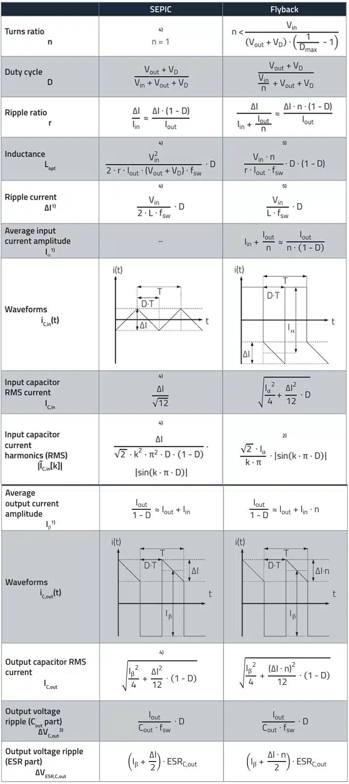
1) These assumptions apply to the ideal switching regulator in continuous conduction mode
(CCM), i.e., the efficiency of the converter is assumed to be 100% (η = 1).
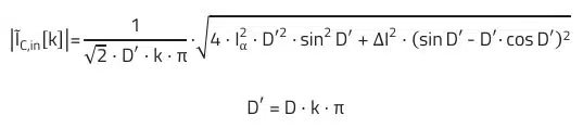
2) The current curve from this equation is approximately rectangular (ΔI neglected). Exactly:
3) The equations defined for ΔVC,out apply to the ideal capacitor. Cout therefore defines the minimum capacitance to meet the ripple voltage requirement. The actual voltage ripple will be higher due to the parasitic inductance ESL (equivalent series inductance) and ESR (equivalent series resistance) of the capacitor.
4) These equations only apply for a coupled choke with a turns ratio of 1:1 (n=1).
5) L corresponds to the main inductance (primary inductance) of the transformer.
FAQ: DC/DC Power Converters
A DC-DC power converter adapts an available DC voltage to the level required by the load and stabilizes it against input voltage variations and load changes, while targeting high efficiency and good EMC behavior. It is used wherever the system supply voltage does not directly match the required operating voltage, such as in battery-powered devices, chargers and renewable energy applications.
A buck converter (step-down) converts a higher input voltage into a lower regulated output voltage, while a boost converter (step-up) raises a lower input voltage to a higher output voltage. Buck-boost topologies such as SEPIC and flyback can generate regulated outputs when the input voltage may be higher or lower than the output and, in the case of flyback, also provide galvanic isolation.
The selection of storage inductors and capacitors is critical because their core material, rated and saturation currents, ESR, impedance and ripple current capability directly influence efficiency, stability and EMC performance. Properly designed input filters and output filters are also essential to meet emission and immunity standards and to control conducted and radiated interference.
A buck converter is typically used when a regulated voltage lower than the input supply is required, for example converting a 24 V bus down to lower logic or subsystem voltages. It behaves like a square-wave generator followed by an LC filter, which requires careful input-side filtering to handle discontinuous currents and EMC constraints.
A boost converter is suitable when the output voltage must be higher than the available input voltage, such as powering higher-voltage rails from a battery or low-voltage bus. Its inductor is placed in the input path so the input current is continuous, but the output current is discontinuous and often requires additional output filtering to control ripple and interference.
A SEPIC converter can regulate the output when the input voltage is sometimes higher and sometimes lower than the output, and it naturally limits short-circuit current thanks to its series coupling capacitor. It is attractive for battery-powered systems due to continuous input current and reuse of common boost controller ICs, but efficiency drops at higher output currents and the coupling capacitor must handle high AC current with very low ESR, often realized by multiple X7R MLCCs in parallel.
Flyback converters are popular up to roughly 150 W because they provide galvanic isolation and one or more regulated outputs using a relatively small number of components, which saves cost and PCB area. However, they exhibit discontinuous trapezoidal currents on both input and output and significant common-mode currents due to transformer and layout parasitics, so they usually require both differential and common-mode EMC filtering and carefully selected Y safety capacitors.
The basic formulas for buck, boost, SEPIC and flyback converters describe ideal relationships between input and output voltage, duty cycle, inductor current ripple and output capacitor sizing in continuous conduction mode with 100% efficiency. In practice, parasitic ESR and ESL of components, non-ideal magnetics and finite efficiency cause higher ripple and losses than predicted by the ideal equations.
How to design a basic DC-DC converter stage
- Define input, output and operating conditions
Start by specifying the minimum and maximum input voltage, required output voltage and current, allowable ripple, isolation requirements and efficiency target. These values determine whether a step-down, step-up, non-isolated buck-boost or isolated topology such as flyback is appropriate.
- Select a suitable converter topology
Choose a buck converter when the input voltage is always higher than the desired output, a boost when it is always lower, a SEPIC when it spans both sides of the output level, or a flyback when galvanic isolation or multiple outputs are required. Also consider power level, cost, controller availability and EMC constraints when finalizing the topology.
- Determine switching frequency and control IC
Select a switching frequency that balances magnetic component size, switching losses and EMI performance, based on application requirements and available controllers. Then choose a controller or integrated converter IC that supports the chosen topology, frequency range, protection features and efficiency target.
- Size the inductor or transformer
Use the ideal DC-DC converter equations in continuous conduction mode to calculate the required inductance or primary inductance so that current ripple and peak currents remain within acceptable limits. Select a core material and geometry that support the switching frequency, rated current and saturation margin while keeping losses and temperature rise under control.
- Select input and output capacitors
Dimension the input and output capacitors using ripple current and voltage ripple requirements, then choose technologies with low ESR and adequate voltage rating for the application. For SEPIC and flyback designs, pay special attention to the coupling and output capacitors, which must handle high AC currents and, in isolated designs, comply with safety and insulation standards.
- Design input and output filters for EMC
Analyze which side of the converter carries discontinuous current and add appropriately dimensioned LC or more complex filters to limit conducted emissions and improve immunity. For flyback and other isolated topologies, include common-mode chokes and Y safety capacitors to control common-mode currents and comply with relevant EMC standards.
- Verify performance with calculations, simulation and measurement
Check currents, voltages and losses against component ratings using the basic converter formulas and refine values with circuit simulation. Build and test a prototype to measure efficiency, thermal behavior, ripple and EMC performance, then iterate component selection and layout as needed.