


Samtec compiled a list of frequently asked questions about EMI shielding and connectors.
Do shielded connectors and cable assemblies help reduce emissions and improve the immunity of electronic products?
Yes, they can help, and in some cases, they can help dramatically. Signals with periodic switching, such as clock lines, are classic noise sources. If energy from this type of source couples to a cable that exits a shielded enclosure, the cable can radiate the coupled noise much like a cell phone antenna radiates (although not as efficiently).
Placing a shield over the cable (and terminating the shield properly) can dramatically reduce the radiated emissions. The situation is similar for a board-to-board connector inside an enclosure, except the radiated emission occurs inside the enclosure, so the radiated emission may or may not be visible during an EMI test.
Do Samtec connectors meet FCC Class B EMI Requirements?
No. Federal standards require EMI compliance testing of active electronic systems such as computers (FCC 47 CFR Part 15, EN55022, etc.). While passive components can impact the overall system-level EMI performance, it is not possible to directly test a connector, cable assembly, resistor, or bolt for EMI compliance.
What are the best practices to reduce EMI when using a board-to-board (BTB) connector?
There are a few assumptions that need to be stated up front before we get into answering this question:
- We are primarily interested in digital applications with kbps to Gbps data rates, not low-frequency analog (audio) applications.
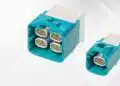
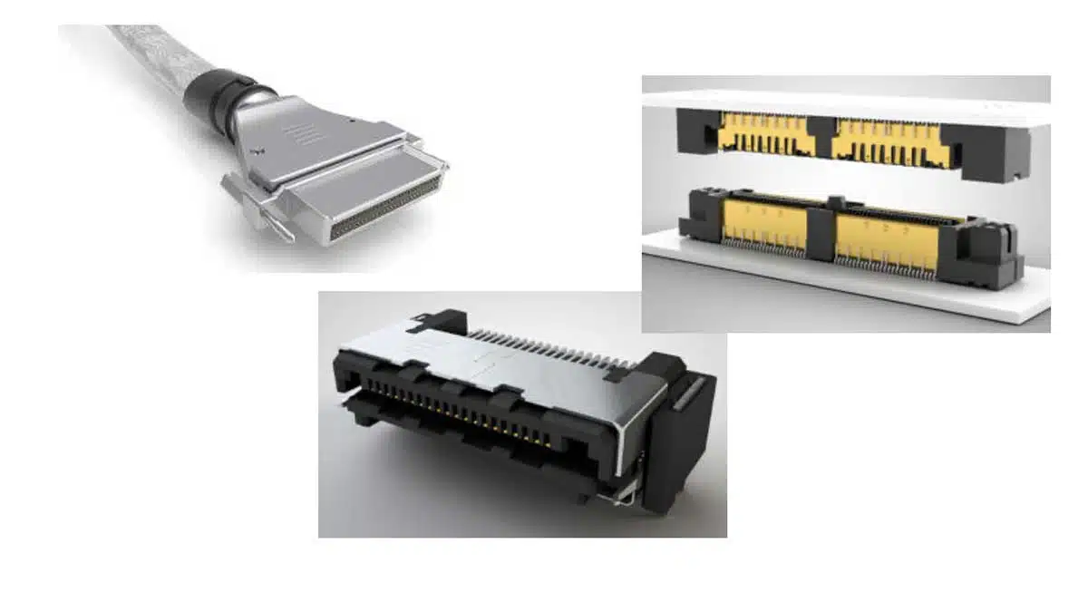
- We address open pin field connectors like the Samtec SEAM/SEAF or QSE/QTE products, not a coaxial RF connector configured for board-to-board applications.
- The connectors are part of an overall interconnect system that can include printed circuit boards (PCBs).
Understanding the radiation mechanism or dominant EMI antennas in a board-to-board system is essential. One effective analogy is to consider the PCB ground planes as elements of a microstrip patch antenna.
Any longitudinal voltage potential developed across the connector appears as a voltage source that drives the PCB ground planes, not unlike a feed element driving a microstrip patch antenna. This is a useful low-frequency (50 MHz to 100 MHz+) approximation; the radiating system is more complex at higher frequencies, but the best practices remain the same.
To minimize the longitudinal voltage potential across a connector, we need to minimize the self-partial inductance of the signal return path. To make sure we’re on the same page, here are three terminology clarifications:
- Loop inductance is the only inductance that is “real” or can be measured.
- Self-partial inductance is a useful mathematical construct; it can be calculated but not directly measured.
- “Self” means we are interested in the magnetic flux developed from only one conductor of the loop.
- “Partial” means we are looking at only a portion of the path, specifically the portion between the PCBs.
To minimize the self-partial inductance across the connector, here are some general principles to follow:
- A short board-to-board stack height is better than a taller one.
- Minimize the connector’s loop area by integrating ground pins into the signal pin field (1:1).
- Use broad, flat conductors for signal return; dedicated planes are superior to pins for signal return.
- Make the characteristic impedance of the signal and ground pattern as low as possible.
If EMI were the only issue, the board-to-board connector should have a very low characteristic impedance (< 1Ω). Planar distribution for signal and return currents would have the lowest self-partial inductance across the connector and the lowest EMI. This is not a practical guideline as data transmission requirements dictate a close match to the system impedance (typically 50Ω).
The same physics that applies to EMI reduction in board-to-board connectors also applies to PCBs. Disruptions in the signal return path, such as splits in the ground plane, drastically increase the self-partial inductance of the return path, which can lead to EMI problems.
The best EMI strategy for electronics considers multiple areas such as PCB design (stack up and circuit layout), connector selection, signal return management (grounding), power filtering (decoupling/PI design), and logic selection with an emphasis on spread spectrum clocking and edge shaping.