Passive Components Blog
No Result
View All Result
  • Home
  • NewsFilter
    • All
    • Aerospace & Defence
    • Antenna
    • Applications
    • Automotive
    • Capacitors
    • Circuit Protection Devices
    • electro-mechanical news
    • Filters
    • Fuses
    • Inductors
    • Industrial
    • Integrated Passives
    • inter-connect news
    • Market & Supply Chain
    • Market Insights
    • Medical
    • Modelling and Simulation
    • New Materials & Supply
    • New Technologies
    • Non-linear Passives
    • Oscillators
    • Passive Sensors News
    • Resistors
    • RF & Microwave
    • Telecommunication
    • Weekly Digest

    5th PCNS Conference Registration Now Open!

    YAGEO Introduces Automotive Supercapacitors for Stable BMS in EVs

    Capacitance Definition of Non-Linear Voltage Dependent Capacitors

    Littelfuse Releases Harsh Environment Robust Tactile Switches

    Bourns Releases Noise Suppression Common Mode SMD Inductors

    Passive Electronic Components Lead-times Update

    Bourns Releases New SMD Line Filter for Enhanced EMI Suppression

    TDK Expands 3-terminal Automotive SMD Chip Filters to 35V

    Quantic Eulex Presents Ceramic Gap RF Capacitors

    Trending Tags

    • Ripple Current
    • RF
    • Leakage Current
    • Tantalum vs Ceramic
    • Snubber
    • Low ESR
    • Feedthrough
    • Derating
    • Dielectric Constant
    • New Products
    • Market Reports
  • VideoFilter
    • All
    • Antenna videos
    • Capacitor videos
    • Circuit Protection Video
    • Filter videos
    • Fuse videos
    • Inductor videos
    • Inter-Connect Video
    • Non-linear passives videos
    • Oscillator videos
    • Passive sensors videos
    • Resistor videos

    Coupled Inductors Circuit Model and Examples of its Applications

    Inductor Resonances and its Impact to EMI

    Highly Reliable Flex Rigid PCBs, Würth Elektronik Webinar

    Causes of Oscillations in Flyback Converters

    How to design a 60W Flyback Transformer

    Modeling and Simulation of Leakage Inductance

    Power Inductor Considerations for AI High Power Computing – Vishay Video

    Coupled Inductors in Multiphase Boost Converters

    VPG Demonstrates Precision Resistor in Cryogenic Conditions

    Trending Tags

    • Capacitors explained
    • Inductors explained
    • Resistors explained
    • Filters explained
    • Application Video Guidelines
    • EMC
    • New Products
    • Ripple Current
    • Simulation
    • Tantalum vs Ceramic
  • Knowledge Blog
  • Suppliers
    • Who is Who
  • Events
No Result
View All Result
Passive Components Blog
No Result
View All Result

Hermetic Glass Micro Bonding for Medical Miniaturization

27.8.2020
Reading Time: 6 mins read
A A
A side-by-side comparison showing a typical medical implant (right) and an implant using a SCHOTT Primoceler all-glass technology (left); Image courtesy of SCHOTT Primoceler

A side-by-side comparison showing a typical medical implant (right) and an implant using a SCHOTT Primoceler all-glass technology (left); Image courtesy of SCHOTT Primoceler

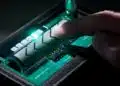
A laser-based process can be used to create ultra-miniaturized hermetic packaging for highly sensitive electronics in demanding applications.

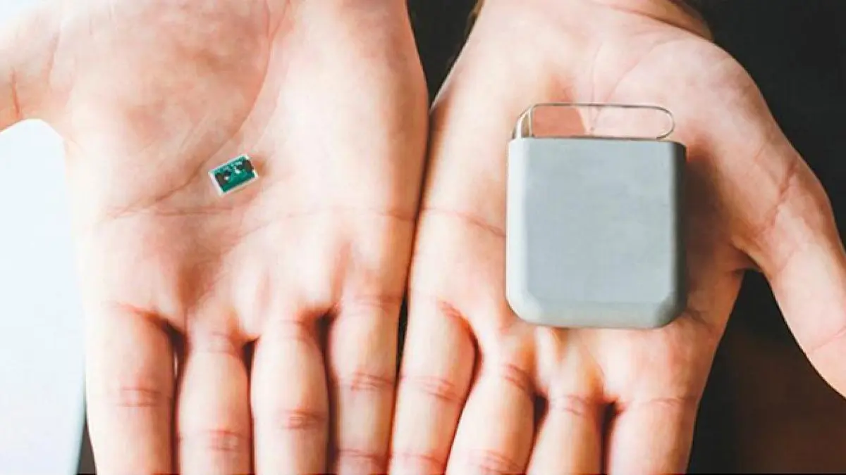
In the medical device industry, recent advancements in increased miniaturization have unlocked a suite of new applications. However, as devices get smaller, it becomes more difficult to create vacuum-tight hermetic seals that protect sensitive electronic parts from damaging elements like moisture, heat, vibrations, and pressure.

RelatedPosts

5th PCNS Conference Registration Now Open!

YAGEO Introduces Automotive Supercapacitors for Stable BMS in EVs

Capacitance Definition of Non-Linear Voltage Dependent Capacitors

A new sealing technology known as Glass Micro Bonding has been developed to enable miniaturization in hermetic packaging. This technology enables the development of next-generation devices with entirely new features, such as full transparency for advanced optical functions as well as completely wireless signal transmission. 

The Limits of Traditional Sealing Technology

Manufacturers of electronic assemblies generally have two vastly different technologies available when sealing their components: they use either adhesive-based bonding or hermetic bonding.

Adhesive-based sealing uses glue, epoxy, or injection molding to create a seal. The advantage of this process is that it can take place at room temperature. However, the organic nature of these adhesives makes the seals non-hermetic and therefore mostly unsuitable for long-term protection. Simply put, they can wear out over time, especially in harsh conditions. This typically rules out adhesive-based bonding in medical applications, where reliability is critical.

In contrast, hermetic bonding uses only inorganic materials such as glass, metal, or ceramics, creating a truly hermetic and vacuum-tight seal. Direct hermetic bonding creates a durable solution for reliability-critical applications. Commonly known hermetic sealing technologies like glass-to-metal and ceramic-to-metal sealing are extremely effective at creating reliable vacuum-tight seals, but simultaneously carry certain size limitations when it comes to miniaturization. While it is possible to create hermetic seals using these technologies that are as small as a few millimeters, the demand for extreme miniaturization and the need for additional functionality (such as digital connectivity) are pushing the limitations of existing processes.

Miniature Wafer-Level Bonding for Medical Applications

Glass Micro Bonding is a wafer-level process that allows the reliable packaging of even miniaturized electronics or MEMS by directly bonding two or more glass wafers without any interface materials. The all-glass wafer-level chip-scale packaging (WLCSP) technology unlocks significant potential in many intriguing applications, including medical implants, 3D MEMS packaging, and other reliability-critical electronic and optical devices.

Glass Micro Bonding entails using an extremely precise laser to fuse glass to glass by melting only the cross section where the glass meets—an area of just a few microns—while leaving all other surfaces untouched. The extremely small and precise seal areas add negligible bulk to the electronic components. This one-step manufacturing process does not require any type of adhesive or additive materials and forms a true direct hermetic seal between the glass wafers.

Glass Micro Bonding diagram miniaturization
Above: An explosion view diagram of a device encapsulated with Glass Micro Bonding. courtesy of SCHOTT Primoceler

The extremely small and isolated area heated by Glass Micro Bonding to form the seal allows even the most heat-sensitive electronics and sensors to be vacuum-sealed in an all-glass hermetic package at room temperature. This opens new doors for Glass Micro Bonding to be used for hermetic sealing in microfluidic devices or sensors that may contain a sensitive organic layer or coating applicable to their specific function.

Ideal for Future Medical Miniaturization Applications Today

Because Glass Micro Bonding does not use any additive materials, it can be performed with new glass types that offer excellent biocompatibility. This makes it particularly ideal for implantable devices, in which biocompatibility is of paramount importance. There is also a decreased likelihood of reactions with other materials that could cause deterioration of component materials and subsequent device malfunction.

While the technology allows for the use of wafers with hermetically sealed through-glass vias, a notable advantage of Glass Micro Bonding is that its transparent glass encapsulation can even eliminate the need for wired connections because radio frequencies (RFs) can travel through the all-glass package. This can reduce both bulk and complexity in device designs while also allowing devices to be Internet-connected, opening the door for live monitoring and firmware updates of implanted devices. Glass Micro Bonding also enables sealed electronics to be combined with chip-based optical components to create optical devices for sensing and imaging, both key functions carried out in the medical treatment landscape.

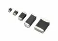
Components sealed with this new technology can be as small as a few cubic millimeters. The technique is very flexible and can be performed on a chip-scale all the way up to wafers as large as 12 inches, making it simple and economical to scale up for high-volume manufacturing.

Real-World Uses

Glass Micro Bonding has been successfully deployed in the industry, with significant research being conducted by companies developing products in both the medical and aerospace industries where failure is not an option.

Glass Micro Bonding nonmagnetic implant miniaturization
Above: An example of a non-magnetic implant sealed with Glass Micro Bonding technology. Image courtesy of SCHOTT Primoceler

For example, Israel-based Nano Retina is using Glass Micro Bonding to seal and protect electronics in its NR600 retinal implant device designed to help restore vision in individuals with blindness caused by retinal degenerative diseases. It was key that the sealing technology not only be clear so it can be used in the eye, but also extremely low profile while maintaining strength and reliability. The implantable device, which works with a set of eyeglasses worn by the patient, replaces the functionality of damaged photoreceptor cells in the eye and creates electrical stimulation that activates remaining healthy retinal cells. In March 2020, Nano Retina announced successful preliminary results for the first human trials of the device—a promising step forward in establishing its retinal implant as a potential answer to degenerative vision loss.

JAMM Technologies and IRD Glass have also been working in collaboration with SCHOTT Primoceler on non-magnetic implants encapsulated in miniature all-glass packages sealed with Glass Micro Bonding. Since the process has an extremely small heat-affected zone of just a few microns and can be effectively performed at room temperature, the possibility has been opened to use non-ferrous materials in implant designs that could otherwise not withstand heat-intensive manufacturing processes.

From Concept to Completion

There is high demand for advancements in medical technology that can help push the entire industry forward. Glass Micro Bonding is one such example of a technology that is enabling innovations and overcoming hurdles previously thought to be insurmountable.

The pioneering technology is compatible with a wide variety of glass types, including borosilicate, fused silica, quartz and soda lime glasses, and silicon. Many people see glass as an inherently breakable material and think of using it to protect critical components as counterintuitive. On the contrary, glass assemblies maintain integrity because of their inorganic complexion that is non-porous, non-aging, and resistant to drastic environmental changes. When working with partners, application-specific testing is performed to validate that the assembly will remain durable and intact under the extreme stress. Testing processes include temperature cycling, moisture resistance, high-temperature storage life, mechanical shock and vibration, and leak tightness.

Glass Micro Bonding is helping to create new types of ultra-miniaturized devices that are reliable and well-tested while also offering connectivity through RF transmission. The hermetic seals created with this technology demonstrate proven reliability in extreme environments and have exceptional longevity.

Related

Source: MD+DI

Recent Posts

5th PCNS Conference Registration Now Open!

5.6.2025
2

Exxelia Power Film Capacitors Support Critical Systems Across Various Industries

13.5.2025
33

H2-Assisted Thermal Treatment of Electrode Materials Increases Supercapacitors Energy Density

13.5.2025
14

Researchers Present Hybrid Supercapacitor Zn-Ion Microcapacitors

12.5.2025
40

Littelfuse Unveils High-Use Tactile Switches with 2 Million Cycle Lifespan

9.5.2025
4

Murata and NIMS Built New Database of Dielectric Material Properties

5.5.2025
78

Tariffs Crush Sales Sentiment in April 2025 ECST Results

5.5.2025
112

Würth Elektronik Offers New Power Supplies Development Kit

29.4.2025
48

3D Printing of Passive Components from Manufacturer Perspective

26.4.2025
49

Hybrid Electrochemical Electrolytic Capacitor Provides High Frequency and High Capacitance Performance

25.4.2025
73

Upcoming Events

Jun 24
17:00 - 18:00 CEST

Ultra-Compact and Efficient Switched-Capacitor Power Converters

View Calendar

Popular Posts

  • Buck Converter Design and Calculation

    0 shares
    Share 0 Tweet 0
  • Boost Converter Design and Calculation

    0 shares
    Share 0 Tweet 0
  • Flyback Converter Design and Calculation

    0 shares
    Share 0 Tweet 0
  • What is a Dielectric Constant and DF of Plastic Materials?

    4 shares
    Share 4 Tweet 0
  • LLC Resonant Converter Design and Calculation

    0 shares
    Share 0 Tweet 0
  • Ripple Current and its Effects on the Performance of Capacitors

    3 shares
    Share 3 Tweet 0
  • SEPIC Converter Design and Calculation

    0 shares
    Share 0 Tweet 0
  • Dual Active Bridge (DAB) Topology Explained

    0 shares
    Share 0 Tweet 0
  • How to Design an Inductor

    0 shares
    Share 0 Tweet 0
  • Flying Capacitors Explained

    0 shares
    Share 0 Tweet 0

Newsletter Subscription


Passive Components Blog

© EPCI - Leading Passive Components Educational and Information Site

  • Home
  • Privacy Policy
  • EPCI Membership & Advertisement
  • About

No Result
View All Result
  • Home
  • Knowledge Blog
  • Premium Suppliers

© EPCI - Leading Passive Components Educational and Information Site

This website uses cookies. By continuing to use this website you are giving consent to cookies being used. Visit our Privacy and Cookie Policy.
Go to mobile version