




A bypass capacitor provides a local, low-impedance path for unwanted supply-current variations and helps stabilize the voltage at an integrated circuit. This article explains its operating principle, frequency limits, PCB placement and selection criteria for design engineers, with practical checks for component engineering and purchasing.
This article develops the original explanation by Jordan Yates of Knowles Precision Devices, with additional guidance on real-capacitor behavior, power-distribution networks and design validation.
Key Takeaways
- A bypass capacitor connects between a supply rail and its local return, supplying transient current and reducing the propagation of supply noise.
- Capacitance alone does not determine performance: effective capacitance, ESR, ESL and PCB mounting inductance all matter.
- Keep the complete capacitor-to-IC power and return loop short and low in inductance, rather than considering physical distance alone.
- Class 2 MLCC capacitance changes with operating conditions; compare manufacturer data at the actual DC bias and temperature.
- Parallel capacitors and ferrite-capacitor networks can introduce resonance peaks. Check the combined network and the regulator’s stability requirements.
- Bypassing supports power integrity but does not replace shielding, appropriate return paths or dedicated transient protection.
Why Are Bypass Capacitors Necessary?
Electronic circuits need supply voltages that remain within their operating limits during both steady operation and changing load demand. Supply noise can enter from outside the circuit or be generated by the circuit itself; local bypassing helps control both mechanisms. [1]
External interference and internal switching currents
Electromagnetic interference can originate from power lines, radio transmitters, electric motors and relay switching. Electrostatic discharge and lightning-related disturbances are additional transient threats, but they require a protection strategy beyond ordinary IC supply bypassing.
- Power-line emissions can couple into wiring and PCB structures.
- Radio transmitters can couple energy into cables, traces and sensitive circuit nodes.
- Motors and relays can generate conducted and radiated switching disturbances.
- Electrostatic discharge and lightning-related transients can exceed component voltage and energy limits.
Supply traces and cables have resistance and inductance, while their geometry also permits capacitive and magnetic coupling. They should not simply be described as inductors that absorb interference. Internally, digital switching and switched analog circuitry draw transient currents that produce voltage disturbances across the impedance of the power-distribution network. [1, 3]

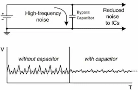
Figure 1 illustrates unwanted variation superimposed on a DC supply. A disturbance associated with the power-line frequency may also contain faster edges and higher-frequency components. The relevant noise spectrum, coupling path and supply impedance must be established before selecting a remedy: a small local bypass capacitor is not a general solution for low-frequency supply ripple.
Supply disturbances can reduce digital noise margins, increase timing uncertainty or introduce errors into analog measurements. Severe electrical overstress can cause latch-up or permanent damage. Bypassing reduces some supply disturbances, but it does not guarantee immunity to these failure mechanisms. [1]
Bypass versus decoupling
The terms bypass capacitor and decoupling capacitor often describe the same physical component from different perspectives. Bypassing emphasizes diverting unwanted AC current through a local path. Decoupling emphasizes reducing interaction between circuits sharing a supply and providing local transient current. [1, 3]
Local capacitors support fast current changes at the device. Bulk capacitance supports slower changes and helps replenish the local capacitors. Their roles overlap, and the required values depend on the IC, the power source and the impedance between them; there is no universal capacitor value or fixed bulk-to-local ratio for every design.
How a Bypass Capacitor Mitigates EMI
A bypass capacitor is normally connected in parallel with the load, between its supply and local return. It exchanges charge as the supply voltage changes and provides a lower-impedance path for selected AC components than the longer path back to the source. Its effectiveness is therefore a property of the complete circuit, not the capacitor alone. [1, 3]
Charge storage and the dielectric
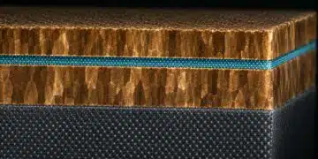
A capacitor consists of conductive electrodes separated by a dielectric, as illustrated in Figure 2. Energy is stored in the electric field. When the local supply tends to fall, the capacitor can supply charge to the load; when the voltage rises, it can accept additional charge. The amount of voltage change depends on capacitance, current and time. [2]

Normal bypass operation does not require charge carriers to cross the insulating dielectric. Changing electric field produces displacement current, while real capacitors also have a small leakage current. Dielectric breakdown is a fault condition, not the mechanism by which a bypass capacitor removes noise.
A capacitor can absorb charge from a brief disturbance, but it is not a voltage clamp. Its voltage can still rise beyond the load’s permissible limit. Select dedicated protection where the expected transient exceeds the voltage, current or energy capability of the bypass network.
Capacitive reactance
For an ideal capacitor, the magnitude of capacitive reactance XC, in Ω, is given by Eq. (1), where f is frequency in Hz and C is capacitance in F. [1, 2]
Eq. (1) shows why increasing capacitance reduces ideal capacitive reactance at a given frequency. As frequency approaches zero, the reactance approaches infinity: after charging, an ideal capacitor draws no steady DC current. The load receives DC through the supply conductor, not through the bypass capacitor. Real capacitors have finite insulation resistance and therefore some leakage.
Figure 3 illustrates the intended reduction in supply variation. However, solving Eq. (1) for frequency does not establish a complete filter’s attenuation or select a narrow rejection band. Attenuation also depends on source and load impedances, connection parasitics and any other filtering components.
ESR, ESL and self-resonance
A useful first-order model adds equivalent series resistance RESR, in Ω, and equivalent series inductance LESL, in H, to the capacitance. Ignoring leakage for the AC analysis, the capacitor’s complex impedance ZC, in Ω, is approximated by Eq. (2), where j is the imaginary unit. [1, 2]
The capacitive and inductive reactances cancel at the approximate self-resonant frequency fSRF, in Hz, given by Eq. (3). Near this point the series model’s minimum impedance is governed largely by ESR. Above it, inductive behavior becomes increasingly important. [1, 2]
Eq. (3) describes the simplified component model. PCB pads, traces, vias and plane connections introduce additional inductance and alter the mounted response. A capacitor can remain useful above its self-resonant frequency if its impedance is still sufficiently low for the application; self-resonance is not an abrupt filtering cutoff. Use manufacturer impedance data and a model of the actual connection. [3]
PCB Placement and Power-Distribution Networks
Good placement minimizes the inductance of the complete current loop between capacitor, supply pin and return pin. A capacitor that looks close to an IC can still perform poorly if its return connection is long or its vias connect through an unfavorable stackup. [1, 3]
Minimize the complete loop
- Follow the IC manufacturer’s recommended decoupling topology and evaluation-board layout where applicable.
- Use short, wide connections between the capacitor and the relevant supply and return structures.
- Place plane-connection vias close to the capacitor pads and consider multiple vias where they reduce the effective connection inductance.
- Consider the distance to the reference plane and the complete PCB stackup, not just the surface trace length.
- Keep sensitive analog and RF supply-return paths consistent with the device’s recommended layout; avoid introducing shared connection impedance unnecessarily.
These are board-level principles. Very fast digital systems and package-level power delivery require a broader power-integrity analysis that includes package and plane behavior; a simple local capacitor model is not sufficient across every frequency. The TI layout training cited here specifically addresses mixed-signal board design, rather than providing a universal processor power-delivery prescription. [3]
Parallel capacitors and anti-resonance
Do not assume that adding a smaller-value capacitor in parallel always improves high-frequency bypassing. Modern surface-mount capacitors of similar construction and package can have similar ESL despite different capacitance values. Their combination can produce an anti-resonance, an impedance peak between resonances that makes the network less effective over part of the spectrum. [3]
Different capacitor technologies and values can still be necessary to cover local and bulk requirements. Select them as a network, including mounting inductance and damping, rather than as an automatic sequence of decreasing capacitances. Ferrite beads and capacitors also form frequency-dependent networks that may need damping and validation. [1, 3]
Bypass Capacitor Design and Selection Checklist
Start with the load and regulator requirements, then compare components at their operating conditions. Nominal capacitance, package size and voltage rating are necessary identifiers, but they do not establish electrical interchangeability. [2, 4]
Electrical and material selection
- Define the supply rail, allowable voltage variation, load-transient behavior and relevant disturbance frequencies.
- Compare effective capacitance at operating DC bias and temperature, including tolerance and the manufacturer’s applicable aging information.
- Check impedance versus frequency, ESR, ESL and the mounted connection rather than selecting from Eq. (1) alone.
- Check rated voltage against steady supply voltage, ripple and expected transients, using the manufacturer’s derating guidance.
- Where relevant, check ripple-current capability, dissipation, self-heating and the operating-temperature limit.
- Check the regulator’s permitted output capacitance and ESR range, including the combined effect of local and bulk capacitors.
MLCCs are widely used for local bypassing because compact constructions can provide low impedance with low connection inductance. Class 2 dielectrics such as X7R provide relatively high capacitance density, but capacitance changes with bias and temperature. The dielectric designation alone does not specify the effective capacitance on a powered board. [2]
Class 1 ceramics such as C0G provide greater capacitance stability, but may not provide the required bulk capacitance in the available size. Electrolytic and polymer capacitors can complement local ceramics where greater stored charge is needed. Film capacitors serve other combinations of voltage, current, loss and stability requirements; there is no universal ceramic-over-film ranking for all bypass and power applications. [1, 2]
Low ESR is often desirable for local transient support, but minimum ESR is not a universal design objective. Some regulator architectures require an output capacitor within a specified ESR range for loop stability, while other regulators are designed for ceramic capacitors. Follow the particular regulator datasheet and validate the assembled circuit. [4]
Catalog parts, custom parts and qualification
For catalog parts, approve the complete manufacturer part number and compare the operating-condition curves of proposed alternatives. Identical nominal capacitance, voltage rating and package size do not guarantee identical bias behavior or impedance. Retain the relevant datasheet and simulation-model revision in the design record. [2]
Consider specialist or custom constructions when a documented requirement cannot be met with a conventional catalog part. Define the required mounted impedance, footprint, environment and acceptance tests before specifying a special electrode or termination arrangement. A low-inductance component cannot compensate for a high-inductance PCB connection.
- Specify the operating environment and required qualification or screening for the actual application, including automotive, defense or medical use where applicable.
- Review mounting, soldering and board-strain requirements, and assess whether mechanical protection or an alternative termination is needed.
- Confirm supply-chain traceability, approved alternatives and change-notification requirements for production.
- Keep ordinary low-voltage IC bypassing distinct from mains suppression and insulation-barrier applications. Do not treat a standard bypass MLCC as an automatically acceptable safety capacitor.
- Keep bypass selection separate from surge and ESD protection selection; establish the required protection at the circuit and equipment level.
How Bypass Capacitors Improve Reliability in Electronic Systems
Correct bypassing helps a circuit achieve its intended performance by reducing supply disturbances and interaction between functional blocks. The benefit depends on the system’s actual sensitivity; a bypass capacitor does not independently guarantee a particular audio, RF, imaging or lighting result. [1]
- Audio amplifiers: local decoupling can reduce supply-related interference and support transient demand, but does not eliminate distortion from unrelated mechanisms.
- Wi-Fi receivers and transmitters: supply integrity supports RF and mixed-signal operation, but data rate and reception also depend on the RF design and operating environment.
- MRI RF pulse-generation electronics: bypassing supports local supply integrity; pulse accuracy and equipment compliance require validation of the complete system.
- Analog-to-digital converters: appropriate supply decoupling helps limit supply-related spurious signals and conversion errors.
- Microcontrollers: local transient-current support helps keep the supply within its permissible operating range during switching activity.
- LED lighting: local bypassing can address fast disturbances in drivers and control circuits, but low-frequency flicker or energy-storage limitations require separate analysis.
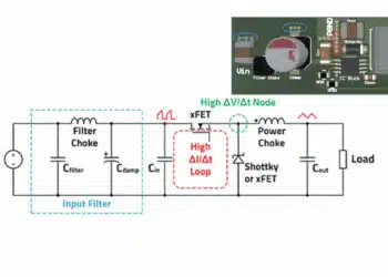
Each application has different noise sources, susceptibility and power demands. Combine bypassing with suitable return paths, shielding, filtering and protection. In switching power supplies, also follow the controller’s input-loop, output-filter and compensation requirements rather than transferring small-signal IC bypass rules without qualification.
Validate the assembled design
Check supply behavior at the relevant device connections under representative switching and load conditions. Compare the measured excursions with the device’s permitted supply range, and investigate ringing or unexpected spectral peaks. Load-transient testing is particularly important where the capacitor network interacts with regulator stability. [1, 4]
Use manufacturer capacitor models and include PCB connection parasitics when simulating the network. Recheck the design when a substitution changes effective capacitance, impedance or mounting geometry. A schematic-level match is not sufficient evidence of equivalent bypass performance. [2, 3]
Conclusion
A bypass capacitor works by providing local transient charge and a controlled AC-current path between a supply and its return. Its practical value comes from the combination of effective capacitance, frequency-dependent impedance and low-inductance mounting.
Select and validate the complete network, including bulk capacitance, regulator compatibility and protection requirements. This approach is more reliable than choosing a nominal value alone or assuming that adding more capacitors always improves the result.
FAQ
A bypass capacitor connects between a supply rail and its local return near a circuit load. It supplies transient current and provides a local path for unwanted AC current. Its effectiveness depends on capacitance, frequency-dependent impedance and the inductance of its PCB connections, not simply its nominal capacitance.
The terms often refer to the same component. Bypassing emphasizes giving unwanted AC current a local alternative path. Decoupling emphasizes reducing interaction between circuits sharing a supply and supporting transient demand. Local and bulk capacitors perform complementary roles, with their values determined by the load, supply and connection impedance.
Start with the IC and regulator recommendations, the permitted supply variation and the load behavior. Compare effective capacitance at operating bias and temperature, then examine impedance over the relevant frequency range. Include PCB inductance, bulk capacitance and possible resonance peaks. Validate the combined network rather than relying on ideal capacitive reactance alone.
Place the capacitor so that its complete connection loop to the relevant supply and return pins has low inductance. Use short, wide connections and suitable nearby plane vias. Physical proximity helps, but the return path, PCB stackup and shared connection impedance also matter. Follow the device manufacturer’s layout guidance.
MLCCs can provide low impedance in compact surface-mount packages with short connections. Their performance depends on dielectric, construction and operating conditions. Class 2 ceramics provide relatively high capacitance density but change with bias and temperature. Compare actual component curves and mounting requirements rather than assuming all MLCCs with the same nominal value are interchangeable.
A bypass capacitor can absorb some transient charge, but it does not clamp voltage to a defined safe level. Its voltage can still exceed the load or capacitor rating. Normal operation does not involve conduction through the dielectric. Assess expected disturbances separately and provide suitable protection where the bypass network is insufficient.
How to Select and Validate a Bypass Capacitor
Select and validate a board-level bypass capacitor as part of the complete supply network.
- Identify supply requirements and disturbances
Record the IC and regulator recommendations, operating rail, permitted voltage variation and load behavior. Distinguish external interference from internally generated switching currents and separate transient protection requirements.
- Compare capacitors at operating conditions
Check effective capacitance at DC bias and temperature, voltage rating, tolerance and relevant aging data. Compare impedance, ESR and ESL over the disturbance frequencies rather than selecting from nominal capacitance alone.
- Minimize the power and return loop
Place the capacitor near the relevant device connections using short, wide conductors and suitable plane vias. Review the complete current loop and PCB stackup against the device manufacturer’s layout guidance.
- Check the complete capacitor network
Include bulk capacitance, mounting parasitics and any ferrite beads in the analysis. Check for impedance peaks and confirm that the combined capacitance and ESR satisfy the regulator’s requirements.
- Validate and document the assembled design
Test representative load and switching conditions, compare supply excursions with device limits and investigate ringing. Record approved part numbers, operating-condition data and qualification requirements, then reassess substitutions that change network behavior.
Further Reading
These related articles provide additional background on capacitor construction, losses and specialist bypass arrangements.
- MLCC and Ceramic Capacitors: background on ceramic dielectric classes, construction and operating limitations.
- ESL Capacitor Parasitic Inductance: further discussion of inductance, packaging and mounting effects.
- Capacitor losses and equivalent series resistance: background on capacitor loss parameters and their interpretation.
- What Is X2Y Bypass Capacitor and What Is It Good For?: an introduction to a specialist electrode arrangement for bypass and filtering applications.
References
The following technical documents support the operating principles and design guidance cited in the article.
- Analog Devices, MT-101: Decoupling Techniques, Analog Devices, 2009.
- Murata Manufacturing, Basics of Ceramic Capacitors: Introduction to MLCC Components in Circuits, Role and Function, Murata Manufacturing, 2024.
- Art Kay, Decoupling Capacitors, TI Precision Labs: ADCs, Texas Instruments, 2022.
- Jeff Falin and John Cummings, ESR, Stability, and the LDO Regulator, SLVA115A, Texas Instruments, revised 2020.
Latest technical review and revision: November 3, 2026. Updated capacitor operating principles, impedance and layout guidance, component selection, FAQ and validation procedure.