Passive Components Blog
No Result
View All Result
  • Home
  • NewsFilter
    • All
    • Aerospace & Defence
    • Antenna
    • Applications
    • Automotive
    • Capacitors
    • Circuit Protection Devices
    • electro-mechanical news
    • Filters
    • Fuses
    • Inductors
    • Industrial
    • Integrated Passives
    • inter-connect news
    • Market & Supply Chain
    • Market Insights
    • Medical
    • Modelling and Simulation
    • New Materials & Supply
    • New Technologies
    • Non-linear Passives
    • Oscillators
    • Passive Sensors News
    • Resistors
    • RF & Microwave
    • Telecommunication
    • Weekly Digest

    Top 10 Connector Vendors by Product Type

    Bourns Releases High‑Q Air Coil Inductors for RF Aplications

    CMSE 2026 Announces Call for Presentations on High-Reliability Military and Space Electronics

    ESA Call for Papers 6th Space Passive Component Days – SPCD 2026

    Würth Elektronik Offers Halogen‑Free EMC Gaskets for Displays and Housings

    Component Distribution Supply Chain January 2026

    Binder Unveils M8 Flange Solder Connectors for Flexible Cabling

    Power Electronics Tools for Passives and Magnetic Designs

    Modelithics Releases Component Model Library for SIMULIA CST Studio Suite

    Trending Tags

    • Ripple Current
    • RF
    • Leakage Current
    • Tantalum vs Ceramic
    • Snubber
    • Low ESR
    • Feedthrough
    • Derating
    • Dielectric Constant
    • New Products
    • Market Reports
  • VideoFilter
    • All
    • Antenna videos
    • Capacitor videos
    • Circuit Protection Video
    • Filter videos
    • Fuse videos
    • Inductor videos
    • Inter-Connect Video
    • Non-linear passives videos
    • Oscillator videos
    • Passive sensors videos
    • Resistor videos

    One‑Pulse Characterization of Nonlinear Power Inductors

    Thermistor Linearization Challenges

    Coaxial Connectors and How to Connect with PCB

    PCB Manufacturing, Test Methods, Quality and Reliability

    Transformer Behavior – Current Transfer and Hidden Feedback

    Choosing the Right Capacitor: The Importance of Accurate Measurements

    RF Inductors: Selection and Design Challenges for High-Frequency Circuits

    Transformer Safety IEC 61558 Standard

    3-Phase EMI Filter Design, Simulation, Calculation and Test

    Trending Tags

    • Capacitors explained
    • Inductors explained
    • Resistors explained
    • Filters explained
    • Application Video Guidelines
    • EMC
    • New Products
    • Ripple Current
    • Simulation
    • Tantalum vs Ceramic
  • Knowledge Blog
  • DossiersNew
  • Suppliers
    • Who is Who
  • PCNS
    • PCNS 2025
    • PCNS 2023
    • PCNS 2021
    • PCNS 2019
    • PCNS 2017
  • Events
No Result
View All Result
Passive Components Blog
No Result
View All Result

How to design a high voltage DCM inverting charge pump converter

7.2.2019
Reading Time: 4 mins read
A A

Source: EDN article

Power Tips #87: How to design a high voltage DCM inverting charge pump converter. By John Betten

RelatedPosts

Top 10 Connector Vendors by Product Type

Bourns Releases High‑Q Air Coil Inductors for RF Aplications

CMSE 2026 Announces Call for Presentations on High-Reliability Military and Space Electronics

A low-current, negative high-voltage is required to bias sensors in advanced driver assistance systems, ultrasonic transducers for sonar applications and communications equipment. Flyback, Cuk and inverting buck-boost converters are all possible solutions, but are penalized by bulky transformers (flyback and Cuk) or limited in their maximum negative voltage by the controller’s input-voltage rating (inverting buck-boost). In this power tip, I’ll detail the operation of a converter that pairs a single inductor with an inverting charge pump operating in discontinuous conduction mode (DCM).  Paired with a ground referenced boost controller, a large negative output voltage can be generated at a lower system cost.

Figure 1 shows a simplified power-stage schematic. Note that this schematic is different from a traditional inverting buck-boost converter, which “floats” the controller between VIN and -VOUT. In that converter, the maximum -VOUT achievable is the maximum VCC of the controller minus the maximum input voltage. This would make it nearly impossible to find a controller that can drive an N-channel field-effect transistor (FET) for an output voltage of -100 V or more.

Figure 1 Simplified power stage of an inductor-driven inverting charge pump.

The circuit’s operation can be split into three intervals, detailed in Figure 2. In the first interval, the FET is on during duty cycle (d), which applies VIN across the inductor, allowing current to ramp up from zero, storing energy. However, in the previous cycle, C1 (which maintains a voltage of approximately equal to VOUT) has depleted its excess stored energy, reverse-biasing D1 and D2. This is why D1, D2 and C1 are not shown in this interval. C2 supplies all load current.

In the next interval, d’, the FET turns off and the inductor current begins to discharge, causing its voltage polarity to reverse. This greatly increases the voltage present at node VFET, allowing C1 to recharge through D1. During this interval, current ramps downward until D1 turns off. However, due to the reverse-recovery characteristics of D1, current goes negative before it eventually turns off, at which point the inductor current slope changes and its voltage polarity reverses once again.

The third interval, d’’, is when the energy transfer from C1 to C2 takes place. When D1 stops conducting, the inductor voltage is clamped to VIN because the VFET node voltage is forced to ground by a current path through the FET’s body diode. Current flows through D2 until the voltages across C1 and C2 equalize, but current through the FET’s body diode continues until the inductor’s current reaches zero. At this point, the voltage across the inductor collapses and resonates with circuit parasitics until the FET turns on again.


Figure 2 The three phases of DCM operation.

Figure 3 details the key voltage and current waveforms. DCM operation allows for the smallest possible inductance, but with a higher peak current. Inductance for DCM operation is determined at the maximum duty cycle, minimum VIN and full load. Carefully check the maximum duty cycle against the controller data sheet, but you can typically choose 60%-90%, or otherwise pulse skipping can occur. Larger inductances will push operation into continuous conduction mode (CCM), since the current will not return to zero before the next switching cycle. This results in using an inductor that may be larger than necessary and requires extra care to prevent subharmonic oscillation.

Figure 3 Key circuit waveforms in DCM.

Design equations

For DCM operation, Equation 1 satisfies the relationship involving the inductor’s stored energy:

where ipk is the peak inductor current and η is the converter’s efficiency. The peak inductor current is then equal to Equation 2:

From the following two equations, Equation 3 expresses the duty cycle (d) in terms of :

Since VIN is the voltage across the inductor when the FET is on and ipk is the inductor current at the end of duty cycle d, substituting Equation 2 into Equation 3 yields Equations 4 and 5:

The average load current is determined by the geometric relationship in Equations 6 and 7 during interval d’:

Substituting Equation 2 into Equation 7 provides Equation 8:


The remainder of the period is defined as d’’, which is when the energy transfers into C2 and the remaining inductor current discharges to zero (Equation 9):

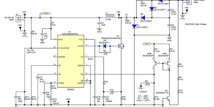
Figure 4 shows an example schematic implementing this converter with a voltage doubler, which allows the voltage stress of each power-stage component to be equal to one-half of the full output voltage. This provides a wider selection of components from which to choose. In this application, the inductance was calculated as if the output voltage was one-half, but at twice the load current.

featured image and Figure 4 Inductor-driven inverting charge pump with voltage doubler and level-shifting current mirror schematic

This converter provides a small, single-inductor solution for generating a large negative voltage. Additionally, it allows the use of an inexpensive ground-referenced boost controller to drive an N-channel FET.

For more Power Tips, check out TI’s Power Tips blog series on Power House.

Related

Recent Posts

Bourns Releases High‑Q Air Coil Inductors for RF Aplications

29.1.2026
19

CMSE 2026 Announces Call for Presentations on High-Reliability Military and Space Electronics

28.1.2026
29

ESA Call for Papers 6th Space Passive Component Days – SPCD 2026

28.1.2026
23

Power Electronics Tools for Passives and Magnetic Designs

27.1.2026
56

Würth Elektronik Developed a Custom Transformer for Active Hand Orthosis

26.1.2026
38

Passive Components in Quantum Computing

22.1.2026
125

Exxelia Offers Custom Naval Transformers and Inductors

21.1.2026
16

Würth Elektronik Introduces Product Navigator for Passive Components

14.1.2026
89

Panasonic Passive Components for Reliable Robotic Arms

14.1.2026
115

Upcoming Events

Feb 24
16:00 - 17:00 CET

Designing Qi2 Wireless Power Systems: Practical Development and EMC Optimization

Mar 3
16:00 - 17:00 CET

Cybersecurity at the Eleventh Hour – from RED to CRA – Information and Discussion

Mar 21
All day

PSMA Capacitor Workshop 2026

View Calendar

Popular Posts

  • Buck Converter Design and Calculation

    0 shares
    Share 0 Tweet 0
  • Boost Converter Design and Calculation

    0 shares
    Share 0 Tweet 0
  • LLC Resonant Converter Design and Calculation

    0 shares
    Share 0 Tweet 0
  • Flyback Converter Design and Calculation

    0 shares
    Share 0 Tweet 0
  • Ripple Current and its Effects on the Performance of Capacitors

    3 shares
    Share 3 Tweet 0
  • How Metal Prices Are Driving Passive Component Price Hikes

    0 shares
    Share 0 Tweet 0
  • MLCC and Ceramic Capacitors

    0 shares
    Share 0 Tweet 0
  • Dual Active Bridge (DAB) Topology

    0 shares
    Share 0 Tweet 0
  • What is a Dielectric Constant and DF of Plastic Materials?

    4 shares
    Share 4 Tweet 0
  • Degradation of Capacitors and its Failure Mechanisms

    0 shares
    Share 0 Tweet 0

Newsletter Subscription


Passive Components Blog

© EPCI - Leading Passive Components Educational and Information Site

  • Home
  • Privacy Policy
  • EPCI Membership & Advertisement
  • About

No Result
View All Result
  • Home
  • Knowledge Blog
  • PCNS

© EPCI - Leading Passive Components Educational and Information Site

This website uses cookies. By continuing to use this website you are giving consent to cookies being used. Visit our Privacy and Cookie Policy.
Go to mobile version