


Thermal management is a challenge for any electronics designer. Among the possible solutions, heatsinks are a key element that aids in heat dissipation. Combining them with thermal materials achieves optimal contact between the component and the cooling device.
This Würth Elektronik video and article explain what a heatsink is for, how to choose one, and the importance of combining it with a thermal interface material.
Heatsinks combined with appropriate thermal interface materials (TIMs) form a passive thermal solution that allows components to operate closer to their full electrical performance while staying within safe junction temperatures.
Key Takeaways
- Heatsinks play a crucial role in thermal management by enhancing heat dissipation from electronic components.
- Effective use of heatsinks requires understanding conduction, convection, and radiation principles for optimal design.
- Thermal interface materials (TIMs) must be properly selected and applied to ensure efficient thermal contact between components and heatsinks.
- Designers should consider the convection regime and mechanical constraints early in the design process to enhance thermal efficiency.
- Choosing the right heatsink involves balancing thermal performance, cost, and weight, often favoring aluminum for standard applications.
Why thermal management matters
More than half of field failures in electronic devices are related to thermal issues rather than purely electrical faults, often because thermal aspects were not considered early enough in the design cycle. If thermal challenges are only discovered at prototype or production stage, the PCB layout is usually frozen and options are limited, forcing larger heatsinks, forced cooling, or costly redesigns.
Elevated temperatures accelerate wear‑out mechanisms in semiconductors and solder joints, and they also introduce mechanical stress through different coefficients of thermal expansion across materials on the PCB. With today’s trend toward compact, high‑performance systems, designers must plan thermal management from the earliest schematic and layout stages to avoid de‑rating components or operating them far below their nominal capability.
Fundamentals of heat transfer in electronics
Effective heatsink use starts with understanding the three main mechanisms of heat transfer from a component to the ambient environment.
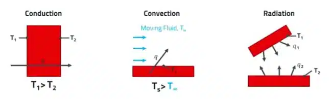
Conduction
Conduction is the transfer of heat through direct contact between solids, for example from a power semiconductor package into a mounted heatsink. The conductive path is characterized by:
- Temperature difference between source and sink.
- Contact area between component case and heatsink base.
- Distance (and air gaps) between surfaces.
- Thermal conductivity of each material in the path.
If the component case and heatsink are at similar temperature, heat flow is negligible. Air gaps and surface roughness significantly increase thermal resistance, which is why a dedicated TIM is typically required between the device and heatsink.
Convection
Convection transfers heat from the heatsink surface into a moving fluid, usually air. Natural convection relies on buoyancy‑driven airflow around the fins, while forced convection uses a fan or system airflow.
Key parameters include:
- Temperature difference between heatsink surface and ambient air.
- Effective surface area exposed to the airflow.
- Convection coefficient, which depends strongly on airflow speed, direction, and the surrounding geometry.
In vacuum, convection is effectively zero, so fans are useless and other mechanisms must dominate. In natural convection, the convection coefficient is relatively low; adding a fan can increase it by an order of magnitude or more, enabling smaller heatsinks or higher power dissipation at a given temperature rise.
Radiation
All bodies with a temperature different from their surroundings radiate energy. For practical heatsink design, radiation is often underestimated but can contribute noticeably, especially at higher temperatures and in natural convection environments.
The radiated heat depends on:
- Temperature difference between heatsink and ambient.
- Surface emissivity of the heatsink material and finish.
Raw or “polished” aluminum has low emissivity; black anodized aluminum has much higher emissivity, approaching a significant fraction of the theoretical maximum. This is why black anodized heatsinks of identical geometry outperform bare aluminum versions: their surface radiates heat more effectively into the environment.
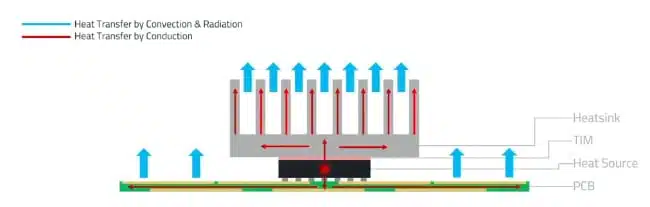
What a heatsink actually does
A heatsink is a passive cooling device that increases the effective surface area for heat transfer from a component into the surrounding air. In a typical arrangement, heat flows:
- From component junction to case.
- Through a TIM layer into the heatsink base (conduction).
- Through the heatsink structure into the fins (conduction and lateral spreading).
- From fin surfaces into air via convection, with an additional contribution from radiation.
Heatsinks do not “destroy” heat; they only facilitate its transfer from a small, highly loaded area (e.g. a TO‑220 tab or BGA package) into a larger area that can effectively couple to the ambient.
Key heatsink design parameters
Base thickness
The base acts as a thermal spreading and storage region between the component and the fins.
- Thicker bases provide more cross‑section for lateral spreading, reduce local temperature gradients, and allow some thermal buffering.
- However, thicker bases increase weight and material cost, and beyond a certain thickness the incremental benefit diminishes.
A practical rule of thumb from the presented data:
- Base thickness around 1–2 mm is generally used for lower‑power applications, roughly in the range of a few watts of dissipation.
- Base thickness around 3 mm and above is more typical for higher‑power applications and larger overall heatsink sizes.
Fin thickness
Fin thickness influences both conduction within the fin and the number of fins that can fit into a given width.
- Thicker fins can carry more heat from the base and contribute more surface area per fin.
- However, thicker fins reduce the number of fins that can fit, which can reduce total surface area if spacing becomes too large.
As a design tip:
- Very thin fins (below roughly 0.5 mm) are generally associated with forced convection applications, where airflow can effectively use high fin density.
- Fins above about 1 mm thickness are more common in natural convection heatsinks, where structural stiffness and manufacturability also play a role.
These rules are not mandatory, but they are useful debugging guidelines when a thermal solution does not meet its target performance.
Fin spacing and thermal boundary layer
Air between fins develops a thermal boundary layer, in which air temperature transitions from the hot fin surface to the cooler bulk air. If fins are too close together, boundary layers can merge, reducing the local temperature difference and hence the rate of heat transfer.
Typical guidance:
- Fin spacing in the 2–4 mm range is common for forced convection with fans, where strong airflow refreshes the air between fins.
- Fin spacing above about 5 mm is more typical for natural convection, helping to avoid excessive boundary layer overlap.
If a heatsink shows poor performance due to boundary layer issues, options include increasing fin spacing or adding forced convection to thin the boundary layer and boost heat transfer.
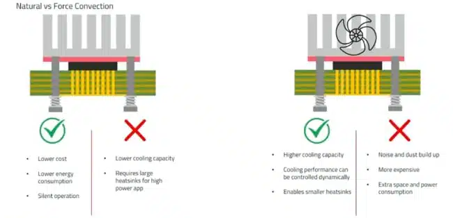
Natural vs forced convection trade‑offs
Forced convection can provide higher cooling capacity and allows dynamic control (e.g. variable fan speed), but introduces additional system cost, noise, dust accumulation, and power consumption. Natural convection requires larger or more efficient heatsinks and often better TIMs, but offers:
- Lower system complexity.
- No fan failures or acoustic noise.
- Reduced power consumption.
For many applications, investing in a slightly larger heatsink and higher‑quality TIM to remain in natural convection can be preferable to adding fans, especially in industrial and maintenance‑sensitive designs.
Thermal interface materials: role and sizing
A thermal interface material fills microscopic and macroscopic gaps between the component surface and the heatsink, replacing air (a poor thermal conductor) with a more conductive medium. Even a well‑machined metal–metal interface has sufficient roughness and flatness variation to justify a TIM in most critical applications.
Why TIM is often the weak link
Application experience shows that designs with good heatsinks and fans can still underperform because of poor thermal contact between component and heatsink. If the TIM is missing, too thick, unevenly applied, or inappropriate for the required gap, thermal resistance increases and the expected junction temperature is not met.
For reliable design, the TIM must be treated as a critical element of the thermal path, not as an afterthought.
Simple method to select TIM performance
The webinar demonstrates a useful engineering approach. For a given component and thermal target:
- Known:
- Power loss of the component, for example .
- Maximum allowed junction temperature for example 85 °C.
- Ambient temperature , for example 60 °C.
- From datasheets:
- Junction‑to‑case thermal resistance .
- Case‑to‑ambient thermal resistance of the heatsink , for the relevant airflow condition.
The thermal path can be modeled as a series resistance network: junction–case, TIM, and heatsink. The total temperature rise is:
Given , , and the known resistances, you can solve this expression for the maximum allowable for the interface material. If the calculated requirement is, for example, 1.3 K/W, you must choose a TIM with equal or lower effective thermal resistance in your actual assembly conditions.
Note that a TIM’s effective thermal resistance depends on:
- Its thermal conductivity.
- Its thickness in the final assembly.
- Actual contact pressure and area.
High conductivity alone does not guarantee low system‑level resistance if the gap is large or the material layer is thick.
TIM selection by gap size
Different TIM families are suited to different gap ranges:
- Thermal pastes and phase‑change materials (PCM): for microscopic gaps and thin bond lines, typically below a fraction of a millimeter.
- Thin pads or films: generally used for small but non‑zero gaps, typical where a fixed mechanical thickness is needed and surfaces are flat.
- Gap fillers: elastomeric or foam‑like materials tailored for larger gaps (several millimeters) that can be compressed to improve contact.
For example, if the gap between PCB and heatsink exceeds several millimeters (e.g. > 5 mm), a compliant gap filler is typically more appropriate than a paste designed for very thin bond lines. Where the gap is very small (e.g. 0.2 mm range), a liquid or phase‑change material is often the more efficient choice.
Electrical isolation and mounting details
For power transistors, the tab or mounting surface is often electrically live. In such cases, the thermal interface stack must provide both thermal conduction and electrical isolation:
- Electrically insulating TIMs (e.g. specific pad materials or ceramic‑filled films) between device and heatsink.
- Insulating bushings around screws to prevent direct electrical contact through the mechanical fasteners.
Neglecting the isolation of screws can undermine an otherwise carefully designed isolation scheme.
Material choice: aluminum vs copper
Copper offers higher thermal conductivity than aluminum, but:
- Is significantly denser and heavier.
- Is considerably more expensive for the same volume.
- Can lead to much higher piece‑part cost for otherwise similar designs.
For many power levels and form factors, aluminum heatsinks with appropriate geometry and surface treatment (e.g. black anodization) provide sufficient thermal performance at a much more attractive cost and weight, making them a logical first choice for standard catalog products.
Transistor heatsinks (TO‑220 / TO‑247)
For through‑hole power transistors, the portfolio includes several aluminum heatsink topologies designed for packages such as TO‑220 and TO‑247:
- Clip‑on heatsinks:
- Can be attached directly to the component without PCB layout changes or screws.
- Suitable for lower power dissipation (around a few watts).
- Offer compact, easy retrofitting or last‑minute integration in designs.
- Simple straight‑fin heatsinks:
- Similar application range as clip‑on parts but typically with somewhat larger surface area.
- Require mechanical fastening, such as a screw, to the component tab.
- Can be added late in the design because they do not require special PCB footprints; they mount on the device itself.
- Curved‑fin heatsinks:
- Use curved fins to increase effective surface area within a similar volume.
- Offer improved thermal performance over simple straight‑fin designs at comparable size.
- Extruded “large” heatsinks:
- Offer the best thermal performance among the presented transistor heatsinks.
- Occupy more PCB area and height; they have mechanical legs that must be planned in the layout from an early design stage.
- Well suited for higher dissipation, on the order of many watts per device where compact solutions are insufficient.
A simulated comparison at 10 W dissipation in a TO‑220 device highlights the performance difference between compact and large profiles, illustrating that undersized heatsinks can lead to unacceptably high device temperatures in demanding conditions.
IC and CPU‑style heatsinks
For ICs, including CPUs, BGAs and small embedded platforms such as Raspberry Pi, the portfolio includes:
- Unidirectional fin heatsinks:
- Optimized for cases where airflow direction is known and dictated by a planned fan or system airflow.
- Allow designers to align fins with the dominant airflow direction for maximum convection efficiency.
- Bidirectional fin heatsinks:
- Offer more flexibility when airflow paths are uncertain or may change (e.g. last‑minute decisions on fan placement).
- Provide reasonable performance regardless of airflow direction and can be used in both natural and forced convection scenarios.
These heatsinks come in multiple sizes to adapt to typical IC footprints and attachment methods.
Pre‑applied TIM variants (HDI / HIC)
To simplify assembly and ensure consistent thermal performance, there are versions of the heatsinks that come with pre‑applied thermal interface materials:
- For IC heatsinks (HIC variants):
- Typically use thermal adhesive tapes.
- Provide both thermal conduction and mechanical attachment to the IC package.
- Reduce assembly steps and variability in TIM application.
- For transistor heatsinks (HDI variants, e.g. for TO‑220/TO‑247):
- Use electrically isolating TIM materials to meet isolation requirements between transistor and heatsink.
- Available both as pre‑assembled combinations (heatsink plus TIM) and as separate components for users who prefer to handle assembly themselves.
These pre‑applied options are especially useful for designers aiming to standardize assembly and reduce the risk of inconsistent thermal performance due to process variation.
Mounting accessories
To provide a complete assembly solution, the portfolio also includes:
- Screws and nuts for mechanical fastening of transistor heatsinks.
- Insulating bushings designed to prevent electrical contact through mounting screws in isolated assemblies.
This helps ensure that the intended electrical isolation between device and heatsink is maintained in real hardware, not just on paper.
Anodization and surface finishing
Many of the heatsinks are black anodized. Anodization is an electrochemical process that modifies the outer surface of aluminum, producing:
- Increased corrosion resistance.
- A more durable surface finish.
- Higher emissivity compared to bare aluminum.
The higher emissivity directly improves radiative heat transfer, which is particularly beneficial in natural convection scenarios. Anodized black is often chosen both for its thermal advantages and its stability under UV exposure, making it a practical default finish for industrial and power electronics environments.
From a thermal standpoint, the color itself is not what matters; rather, the surface treatment associated with a given color determines emissivity and thus influences radiative cooling performance.
Practical design‑in notes for engineers
1. Treat thermal design as a system
When selecting heatsinks and TIMs:
- Consider the full thermal resistance chain from junction to ambient, including the PCB, device package, interface, and heatsink.
- Be cautious when comparing heatsink thermal resistance values from different manufacturers, because there is no universal standard for characterization. Conditions such as mounting, airflow, and test configuration can differ significantly.
Catalog thermal resistance figures are useful for relative comparison of heatsink designs, but final performance must be verified in the real application by measurement and/or detailed simulation.
2. Choose convection regime early
Decide early whether your system will rely on natural convection, forced convection, or a combination:
- Natural convection:
- Prefer larger heatsinks with appropriate fin spacing.
- Invest in high‑quality TIMs and good mechanical interfaces.
- Avoid designing in fans that you might later remove; this can result in under‑cooled systems if the heatsink was chosen assuming forced airflow.
- Forced convection:
- Optimize fin density and orientation to match airflow direction.
- Consider fan reliability, noise, dust, and power budget.
- Provide adequate protection against dust buildup, which can degrade performance over time.
Once this decision is made, it strongly influences heatsink geometry options and mechanical layout.
3. Match TIM to mechanical constraints
Select TIM types based on:
- Gap size between component and heatsink.
- Required electrical isolation.
- Assembly method (screwed, clipped, adhesive).
- Production volume and process capability.
For example:
- For minimal gap between a flat transistor tab and a machined heatsink, an electrically isolating pad or film may be appropriate, potentially supplemented or replaced by a phase‑change material or paste if isolation is not required.
- For larger distances between a PCB and a case‑mounted heatsink, a compressible gap filler that tolerates mechanical tolerances is often a more robust choice than trying to use a very thick layer of paste.
Designers should also be mindful that extremely high‑performance TIMs can be costly; reducing mechanical gap thickness can often enable use of more economical materials without sacrificing thermal performance.
4. Validate with appropriate measurements
When verifying thermal design:
- Use both component‑level temperature measurements (e.g. junction estimates from internal diodes, case thermocouples) and heatsink surface imaging (e.g. thermal cameras).
- Do not rely solely on heatsink surface temperature. A cool heatsink does not guarantee a cool semiconductor, especially if TIM coverage is poor or if the contact area is misaligned.
Thermal cameras are useful diagnostic tools, but they must be used in conjunction with proper knowledge of what is being measured and how it relates to the internal junction temperature.
5. Plan for portfolio evolution and scalability
For scalable product families, it is often beneficial to:
- Standardize on a heatsink footprint and mounting concept that can accommodate multiple power classes.
- Provide space in the design for upgrading from a simple clip‑on heatsink to a larger extruded version if a future variant requires higher dissipation.
- Leave mechanical flexibility for adding or removing a fan, keeping in mind that the heatsink geometry should still function reasonably in both natural and forced convection.
This aligns with the approach discussed in the webinar: rather than always choosing the largest available heatsink, understand the application’s thermal requirements and select the smallest solution that reliably meets them.
Source
This article is based on a Würth Elektronik webinar on heatsink solutions and thermal management in electronic devices, including the presentation of their aluminum heatsink and thermal interface material portfolio. All technical details on specific products, materials, thermal behaviors, and application guidelines are according to the manufacturer’s public information and associated datasheets.
References
- Würth Elektronik – Thermal Management overview
- Heatsink Solutions: Thermal Management in our electronic devices – Würth Elektronik YouTube webinar