Passive Components Blog
No Result
View All Result
  • Home
  • NewsFilter
    • All
    • Aerospace & Defence
    • Antenna
    • Applications
    • Automotive
    • Capacitors
    • Circuit Protection Devices
    • electro-mechanical news
    • Filters
    • Fuses
    • Inductors
    • Industrial
    • Integrated Passives
    • inter-connect news
    • Market & Supply Chain
    • Market Insights
    • Medical
    • Modelling and Simulation
    • New Materials & Supply
    • New Technologies
    • Non-linear Passives
    • Oscillators
    • Passive Sensors News
    • Resistors
    • RF & Microwave
    • Telecommunication
    • Weekly Digest

    ESR of Capacitors, Measurements and Applications

    Murata Christophe Pottier Appointed President of EPCIA

    3-Phase EMI Filter Design, Simulation, Calculation and Test

    YAGEO Unveils Compact 2.4 GHz SMD Antenna

    KYOCERA AVX Releases Antenna for Iridium Satellite IoT Applications

    Molex Releases Industry-First Quad-Row Board-to-Board Connectors with EMI Shields

    Image credit: Samtec

    How to Match the Right Connector with Protocol Requirements

    Smoltek CNF-MIM Capacitors Pass 1,000h Reliability Test

    Capacitor Lead Times: October 2025

    Trending Tags

    • Ripple Current
    • RF
    • Leakage Current
    • Tantalum vs Ceramic
    • Snubber
    • Low ESR
    • Feedthrough
    • Derating
    • Dielectric Constant
    • New Products
    • Market Reports
  • VideoFilter
    • All
    • Antenna videos
    • Capacitor videos
    • Circuit Protection Video
    • Filter videos
    • Fuse videos
    • Inductor videos
    • Inter-Connect Video
    • Non-linear passives videos
    • Oscillator videos
    • Passive sensors videos
    • Resistor videos

    3-Phase EMI Filter Design, Simulation, Calculation and Test

    Transformer Design Optimization for Power Electronics Applications

    Common Mode Chokes Selection for RF Circuits in Next-Generation Communication Systems

    Capacitor Self-balancing in a Flying-Capacitor Buck Converter

    How to Select Ferrite Bead for Filtering in Buck Boost Converter

    Power Inductors Future: Minimal Losses and Compact Designs

    Percolation Phenomenon: Degradation of Molded Power Inductors in DC/DC Converters

    Connector PCB Design Challenges

    Efficient Power Converters: Duty Cycle vs Conduction Losses

    Trending Tags

    • Capacitors explained
    • Inductors explained
    • Resistors explained
    • Filters explained
    • Application Video Guidelines
    • EMC
    • New Products
    • Ripple Current
    • Simulation
    • Tantalum vs Ceramic
  • Knowledge Blog
  • Suppliers
    • Who is Who
  • PCNS
    • PCNS 2025
    • PCNS 2023
    • PCNS 2021
    • PCNS 2019
    • PCNS 2017
  • Events
No Result
View All Result
Passive Components Blog
No Result
View All Result

Parameters of Shielding Attenuation

14.4.2025
Reading Time: 8 mins read
A A

This article provides an overview of shielding parameters such as reflection loss, absorption attenuation or back-reflection attenuation. The post is based on Würth Elektronik‘s “Reference Guide ABC of Shielding” that can be ordered from WE website here. Published under permission from Würth Elektronik.

as an introduction read the previous post: Electromagnetic Housing Shielding and Its Effectiveness

RelatedPosts

Shielding Cabinets

Magnetic Shielding and Magnetic Shielding Sheets

Corrosion its Development and Prevention

Parameters Of Shielding Attenuation

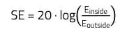
The shielding effectiveness of a housing describes the logarithmic ratio between the field strength without housing and the field strength if the housing is present and is calculated with:

where,

  • SE: Shielding Effectiveness in dB
  • Einside: Field strength without housing
  • Eoutside: Field strength with housing

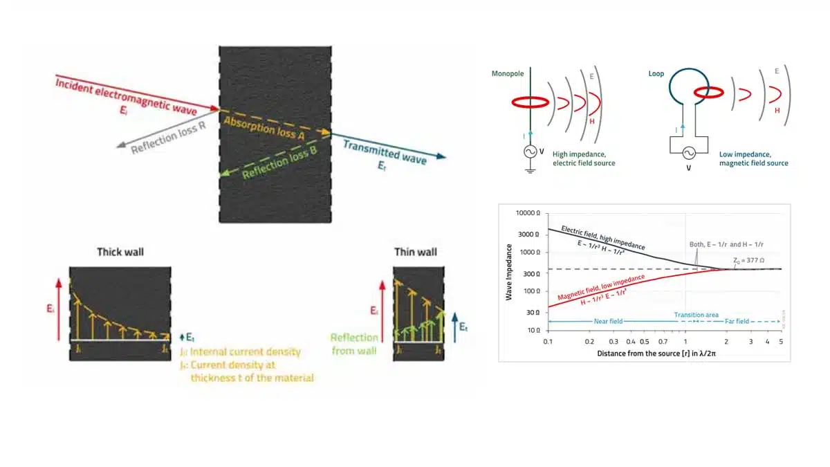
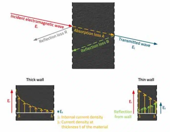
The shielding effectiveness is the sum of the reflection, absorption, and back reflection losses, as shown in Figure 1. and given by the following equation:

S = R + A + B

where,

  • S: Shielding loss in dB
  • R: Reflection loss in dB
  • A: Absorption loss in dB
  • B: Back reflection loss (correction factor in case of thin shielding material) in dB

Figure 1. and equation above shows that, the shielding effectiveness is composed of the reflection loss, the absorption loss, and an additional share of the so-called back reflection losses. The latter only occurs with thin shielding sheets. Details are explained in the following sections.

In this “transmission line model” for shielding attenuation described here, the coupling between the shielding currents and the source of the incident field is neglected. This is no problem for understanding the shielding effect, especially since we will see that the main factors influencing the shielding effectiveness are the housing openings.

Fig. 1.:  Representation of the shielding effectiveness as the sum of the reflection, absorption and back reflection losses.

Reflection Loss R

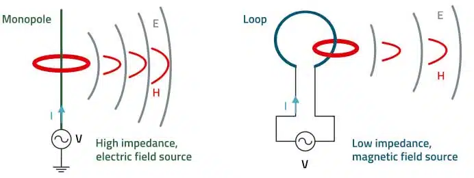
In order to understand the different components of shielding effectiveness, it is necessary to consider the relationship between field sources and source impedances. Two other important factors are the distance between the field (or interference source) and the shielding wall and, if openings in the housing are involved, the polarization of the wave.

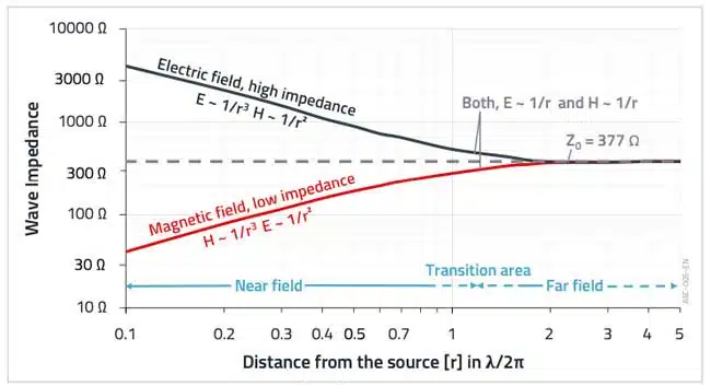
If the field source radiates an electric field (E-field antenna, rod antenna), then the electric field decreases faster (1/r3) than the magnetic field (1/r2) with increasing distance. The wave imped-ance therefore decreases with distance and asymptotically approaches the value Z0 = 377 Ω in the far field. The reverse is true for the situation of a source emitting a magnetic field (ring antenna, loop antenna, H-field antenna), which has a low impedance. This impedance increases with distance, where it asymptotically approaches the value of 377 Ω in the far field. Figure 2. graphically illustrates the definition of the so-called near field and far field ranges of electric, magnetic, and electromagnetic fields.

Fig. 2.: Definition of the near field and far field ranges, graphical representation

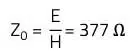
The definition of the near field, the transition area between the near and far fields, and the far field is derived from Maxwell’s equations. Furthermore, the wave impedance of the free space in the far field resulting from the equations is:

where,

  • Z0: Wave impedance of free space in the far field in Ω
  • E: Electric field in V/m
  • H: Magnetic field in A/m

In case r >> λ/2π, the situation is called far field. The far field is also called radiation field because a plane wave prevails in this area.
In case r << λ/2π, the situation is called near field. For this condition, the wave impedance depends on the field-, or radiation source, and is calculated for a high-impedance, i.e., electric field with:
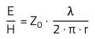
where,

  • r: Distance from the source in m

Relative to Z0 of 377 Ω, the radiation impedance of an electric field is therefore high and that of a magnetic field small. Figure 3. graphically illustrates the impedance conditions of the two field types.

Fig. 3.: Impedance conditions of electric and magnetic fields

The reflection attenuation R, or the reflection loss, depends on the ratio of the wave impedance Z0 of free space to the impedance of the shielding material. The impedance of the shielding ma-terial is a function of its conductivity and permeability, as well as the frequency of the field to be shielded. Materials with high conductivity, such as copper and aluminum, have a higher E-field reflection loss than materials with lower conductivity, such as steel. The reflection loss decreas-es for the E-field (electric) and increases for the H-field (magnetic) with increasing frequency.

In the near field (Figure 2.) the distance between the source and the shield also influences the reflection loss. Near an E-field source, the impedance of the electric field is high, and the reflection loss is correspondingly high. Conversely, near an H-field source, the impedance of the magnetic field is low, and the reflection loss is correspondingly low. In the far field, the wave hit-ting the shield is a plane wave, the wave impedance is constant, and the distance is insignificant.

Absorption Attenuation A

The absorption loss, or absorption attenuation A, depends on the thickness of the barrier and the skin penetration depth and is the same for electric, magnetic, and plane waves. Unlike reflection loss, it does not depend on the wave impedance. The skin penetration depth in turn depends on the properties of the shielding material; steel, for example, offers higher absorp-tion than copper for the same sheet thickness. At high frequencies, absorption becomes the dominant part of the shielding effectiveness and increases exponentially with the square root of the frequency.

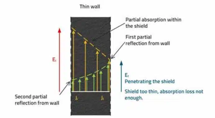
Back-Reflection Attenuation B

The transmitted part of the incident wave continues in approximately the same direction after penetrating the first interface (Figure 4.). The wave is absorbed as it passes through the finite thickness barrier. At the second interface of the barrier, reflection and transmission phenom-ena occur again. The fraction penetrating the barrier is the amount of energy that has passed through the first interface minus the energy that has been absorbed while passing through the barrier and reflected at the second interface. The second reflection, which occurs in the barrier material, contributes only an insignificant amount of energy reduction, and is usually neglected.

The back-reflection attenuation B is, in most cases, insignificant if the absorption attenuation A is greater than 9 dB but becomes important for thin screens at low frequencies.

Fig. 4.: Multiple reflections in thin screens with field penetration

Shielding Attenuation Of Materials In The Far Field (Plane Wave)

The combination of reflection and absorption attenuation results in total shielding effectiveness. The relationships for the shielding effectiveness are shown in Figure 5. and Figure 6. The correction factor B for multiple reflections through thin sheets is neglected here. Since there are many variables, the curves represent the parameters of copper and iron sheets with a thickness of 25 µm, electric and magnetic fields, and plane waves. The source to sheet distance is 5 cm in the near field and 3 m in the “far field”. With the exception of low frequency magnetic fields, the figure shows that the reflection loss is the main damping mechanism at low frequencies, while the absorption loss is the main damping mechanism in the high frequency range.

Fig. 5.: Shielding effectiveness with copper sheet above frequency for electric and magnetic fields and plane waves
Fig. 6.: Shielding effectiveness with sheet iron over frequency for electric and magnetic fields and plane waves

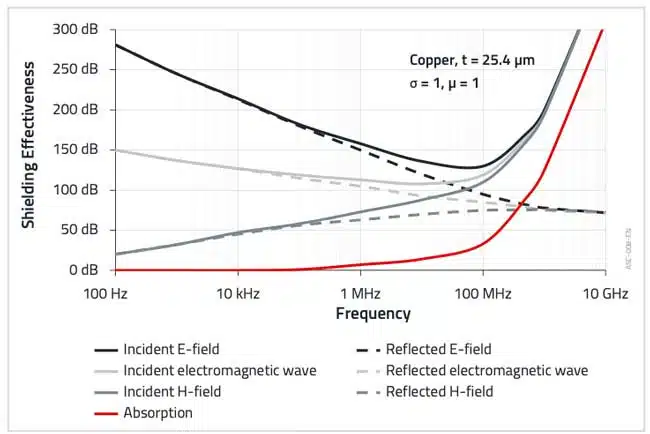
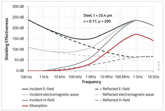
As can be seen in Figure 5. and Figure 6., the material properties have a great influence on the shielding effectiveness. In practice, shielding effectiveness values above approximately 130 dB are no longer measurable. The attenuation values shown graphically in Figure 5. and Figure 6. were determined by calculation and simulation.

Related

Source: Reference Guide ABC of Shielding

Recent Posts

ESR of Capacitors, Measurements and Applications

7.11.2025
2

3-Phase EMI Filter Design, Simulation, Calculation and Test

6.11.2025
19
Image credit: Samtec

How to Match the Right Connector with Protocol Requirements

6.11.2025
8

Transformer Design Optimization for Power Electronics Applications

4.11.2025
14

Microhardness — the Hidden Key to Understanding MnOx Cathode Quality in Tantalum Capacitors

3.11.2025
23

Lightweight Model for MLCC Appearance Defect Detection

3.11.2025
25

Common Mode Chokes Selection for RF Circuits in Next-Generation Communication Systems

30.10.2025
16

Capacitor Self-balancing in a Flying-Capacitor Buck Converter

30.10.2025
45

How to Select Ferrite Bead for Filtering in Buck Boost Converter

23.10.2025
53

Power Inductors Future: Minimal Losses and Compact Designs

30.10.2025
59

Upcoming Events

Nov 11
17:00 - 18:00 CET

Industrial Applications Demand More from Interconnects in Next-Gen Designs

Nov 12
11:00 - 12:00 CET

PCB Design: Impedance is for everyone!

Nov 12
November 12 @ 12:00 - November 13 @ 14:15 EST

Microelectronic Packaging Failure Modes and Analysis

View Calendar

Popular Posts

  • Buck Converter Design and Calculation

    0 shares
    Share 0 Tweet 0
  • Boost Converter Design and Calculation

    0 shares
    Share 0 Tweet 0
  • LLC Resonant Converter Design and Calculation

    0 shares
    Share 0 Tweet 0
  • Flyback Converter Design and Calculation

    0 shares
    Share 0 Tweet 0
  • Ripple Current and its Effects on the Performance of Capacitors

    3 shares
    Share 3 Tweet 0
  • MLCC and Ceramic Capacitors

    0 shares
    Share 0 Tweet 0
  • Dual Active Bridge (DAB) Topology

    0 shares
    Share 0 Tweet 0
  • What is a Dielectric Constant and DF of Plastic Materials?

    4 shares
    Share 4 Tweet 0
  • Flying Capacitors

    0 shares
    Share 0 Tweet 0
  • SEPIC Converter Design and Calculation

    0 shares
    Share 0 Tweet 0

Newsletter Subscription


Passive Components Blog

© EPCI - Leading Passive Components Educational and Information Site

  • Home
  • Privacy Policy
  • EPCI Membership & Advertisement
  • About

No Result
View All Result
  • Home
  • Knowledge Blog
  • PCNS

© EPCI - Leading Passive Components Educational and Information Site

This website uses cookies. By continuing to use this website you are giving consent to cookies being used. Visit our Privacy and Cookie Policy.
Go to mobile version