Passive Components Blog
No Result
View All Result
  • Home
  • NewsFilter
    • All
    • Aerospace & Defence
    • Antenna
    • Applications
    • Automotive
    • Capacitors
    • Circuit Protection Devices
    • electro-mechanical news
    • Filters
    • Fuses
    • Inductors
    • Industrial
    • Integrated Passives
    • inter-connect news
    • Market & Supply Chain
    • Market Insights
    • Medical
    • Modelling and Simulation
    • New Materials & Supply
    • New Technologies
    • Non-linear Passives
    • Oscillators
    • Passive Sensors News
    • Resistors
    • RF & Microwave
    • Telecommunication
    • Weekly Digest

    Samsung Electro-Mechanics Releases High-Capacitance MLCCs for AI Server Applications

    Samsung Electro-Mechanics Releases 165C Automotive 0806 Size Power Inductors

    Coupled Inductors Circuit Model and Examples of its Applications

    Würth Elektronik Introduces LTspice Models for ESD Products

    Capacitor Ripple Current Testing: A Design Consideration

    TDK Releases 0201 High-Frequency Smallest Inductors

    Coilcraft Extends Air Core RF Inductors

    Bourns Releases Automotive 1W Flyback Transformer

    Wk 20 Electronics Supply Chain Digest

    Trending Tags

    • Ripple Current
    • RF
    • Leakage Current
    • Tantalum vs Ceramic
    • Snubber
    • Low ESR
    • Feedthrough
    • Derating
    • Dielectric Constant
    • New Products
    • Market Reports
  • VideoFilter
    • All
    • Antenna videos
    • Capacitor videos
    • Circuit Protection Video
    • Filter videos
    • Fuse videos
    • Inductor videos
    • Inter-Connect Video
    • Non-linear passives videos
    • Oscillator videos
    • Passive sensors videos
    • Resistor videos

    Coupled Inductors Circuit Model and Examples of its Applications

    Inductor Resonances and its Impact to EMI

    Highly Reliable Flex Rigid PCBs, Würth Elektronik Webinar

    Causes of Oscillations in Flyback Converters

    How to design a 60W Flyback Transformer

    Modeling and Simulation of Leakage Inductance

    Power Inductor Considerations for AI High Power Computing – Vishay Video

    Coupled Inductors in Multiphase Boost Converters

    VPG Demonstrates Precision Resistor in Cryogenic Conditions

    Trending Tags

    • Capacitors explained
    • Inductors explained
    • Resistors explained
    • Filters explained
    • Application Video Guidelines
    • EMC
    • New Products
    • Ripple Current
    • Simulation
    • Tantalum vs Ceramic
  • Knowledge Blog
  • Suppliers
    • Who is Who
  • Events
No Result
View All Result
Passive Components Blog
No Result
View All Result

Researchers Proposed Novel 3D Porous Alumina Ta-Nb Oxide Structure for High Energy Electrolytic microCapacitors

3.7.2024
Reading Time: 6 mins read
A A

Researchers from Brno University of Technology; Czech Republic, Tarragona University; Spain and Hokkaido University; Japan proposed novel 3D nanostructured electrodes for capacitors based on porous-anodic-alumina-templated Ta-Nb-alloy/oxide coatings via the magnetron sputtering/anodizing.

Abstract

RelatedPosts

Samsung Electro-Mechanics Releases High-Capacitance MLCCs for AI Server Applications

Samsung Electro-Mechanics Releases 165C Automotive 0806 Size Power Inductors

Coupled Inductors Circuit Model and Examples of its Applications

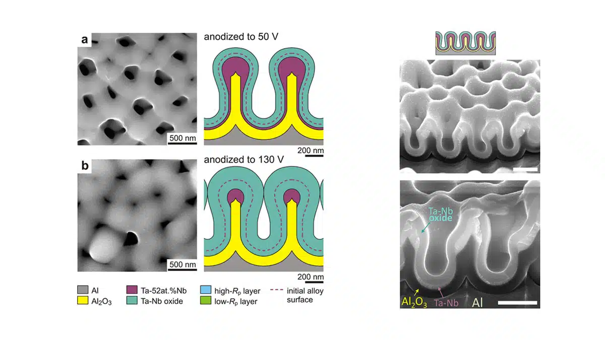
The Ta-52at.%Nb thin alloy films were magnetron sputter-deposited over a low-aspect ratio nanoporous anodic-alumina template formed in 0.05 M tartaric acid solution at 250V and modified by the pore-widening technique to enlarge the pores up to ~500 nm. The alloy coated the pores evenly, thus forming a 3D continuous conducting nanofilm on the template.

Partially anodizing the templated alloy in a borate buffer solution of pH 7.5 generated a compact amorphous mixed-oxide anodic film thickening proportionally to the applied voltage. It was revealed that the oxide on the Ta-52at.%Nb alloy grows with a slower migration of Ta5+ ions relative to Nb5+ ions, resulting in mixing Ta2O5 and Nb2O5 in the film depth and forming a few-nm-thick Nb2O5 outmost layer.

The unique migration of Ta4+, Ta3+, Nb4+, and Nb3+ ions is assumed accountable for forming corresponding suboxides in the 3D anodic film in contrast to a flat Ta-52at.%Nb alloy film used as a reference. The 3D anodic films behave as an n-type semiconductor with a low donor density Nd = ~2×1018 cm−3, appropriate for dielectric applications. An unusual two-layered structure with a sharp electrical interface revealed in the 3D oxide films anodized to 30–130 V, comprising a low resistivity layer superimposed on the high-resistivity layer, is explained by an immobile negative space charge in the outer film part.

The air-annealing at moderate temperatures releases the space charge and transforms the two layers into a high-resistivity single layer having substantially improved dielectric properties and thermostable (up to 250 °C) capacitance of 1.2 uF cm−2 achieved for the film anodized to practical 50 V. The 3D films having up to 4.5 times enlarged effective surface area can be utilized as novel metal/oxide nanostructured electrodes for electrolytic microcapacitors suitable for classical electronic circuits and energy-storage applications.

Introduction and Scope of the Research

Among the various engineered nanostructured materials, 3D nanostructures have become most appropriate for constructing high-performance nano- and microdevices. They seem indispensable for designing electrodes for electrochemical energy conversion and storage devices, including various types of capacitors, which ideally should combine high energy storage and power density.

(a, b) Surface-view SEM images and schematics of corresponding cross-sections of a 3D Ta-52at.%Nb alloy anodized to (a) 50 V and (b) 130 V. (c) Schematic views explaining the impact of annealing and repeated anodizing on the thicknesses of the high-Rp and low-Rp layers in the 3D Ta-52at.%Nb alloy films anodized to 50 V and then 60 V. Source: https://doi.org/10.1016/j.surfcoat.2024.131042

Electrolytic capacitors are particularly suitable in electronic circuits for passing or bypassing signals, noise filtering, or decoupling. Besides, because of their potential for a large specific volumetric capacitance, electrolytic capacitors can store large amounts of energy, substantially overperforming electrostatic capacitors in energy-storage applications and supercapacitors in dealing with current fluctuations. Tantalum and niobium capacitors with its Ta2O5 respcetively Nb2O5 dielectric layers have been proved as one of the most reliable and high energy density capacitor technologies.

In pursuit of energy storage devices and systems smaller and lighter, the development of 3D nanostructured electrolytic capacitors may contribute substantially to the future high-yield production of large-value electrolytic microcapacitors suitable for on-chip integration. It should be noted that the challenge cannot be met with the ALD approach because it is not appropriate for depositing metal layers and any layers thicker than a few nanometers.

In the present work, we have developed an alternative, ALD-unemploying, facile, and highly reproducible technology for 3D nanostructured electrodes for electrolytic microcapacitors that combines the formation of relatively large-nanopore PAA templates with the DC magnetron sputter-deposition of metal or metal-alloy layers and subsequent partial anodizing of the deposit for forming continuous anodic-oxide layers of various thicknesses to serve as the capacitor dielectric.

To this end, we adopted a set of technological, electrical, and electrolytic conditions for forming a low-aspect-ratio PAA template in which the pore population density, pore size, and pore depth were balanced to achieve a substantial rise in the open film surface. Recently, niobium capacitors were developed and became an alternative and competing technology for tantalum electrolytic capacitors.

In the present work, we mixed tantalum with niobium to create a solid solution with approximately equal concentrations of the components, striving to improve the properties of individual metal oxides toward better-quality dielectrics based on previous reports justifying the advantages of such mixing.

For the first time, the Ta-Nb alloy was magnetron-sputter deposited over the PAA template in such a way that it conformally coated the pores, leaving the pore necks unblocked by the deposit and allowing anodizing voltages up to 130 V. The PAA-templated, anodized, and annealed alloy layers were examined by scanning electron microscopy (SEM), X-ray photoelectron spectroscopy (XPS), X-ray diffraction (XRD), electrochemical impedance spectroscopy (EIS), and Mott-Schottky analysis to gain an insight into the formation-structure-property relationship of these unique 3D nanostructures and assess their applicability as the electrodes for electrolytic microcapacitors.

Summary and Conclusions

  1. The Ta-52at.%Nb alloy coatings were magnetron sputter-deposited and partially anodized over a PAA template with 500 nm pores to form high-quality continuous 3D alloy/oxide nanofilms of up to 4.5 times enlarged surface area.
  2. The anodic films grow by migration of cations and anions, with slower migration of Ta5+ ions relative to Nb5+ ions, creating mixed oxides in the film depth. The unusual migration of Ta4+, Ta3+, Nb4+, and Nb3+ ions forms several suboxides in the 3D anodic-oxide nanofilm.
  3. The anodic films behave as an n-type semiconductor with low donor densities Nd = ~2×1018 cm−3, appropriate for dielectric applications.
  4. The two-layered structure revealed for the 3D nanofilms anodized above 30 V transforms into a single high-resistivity (~100 MΩ cm2 nm−1) layer after air annealing at temperatures over 200 °C due to releasing the negative space charge from the outer film part.
  5. The capacitance of the 3D oxide nanofilm formed by anodizing to practical 50 V is 1.2 uF cm−2 and independent of annealing temperature, while the anodic oxide becomes increasingly dielectric with rising annealing temperature above 200 °C.
  6. The coatings developed here may be utilized as novel 3D nanostructured electrodes/dielectrics for electrolytic microcapacitors suitable for traditional electronic circuits and energy-storage applications. Gas-sensing, superhydrophobic, or biomedical effects may also arise in these 3D nanofilms, similar to some previously reported self-organized anodic oxides on valve metals.

Read the complete article under link here:

A. Mozalev, M. Bendova, F. Gispert-Guirado, et al., Porous anodic-alumina-templated Ta-Nb-alloy/oxide coatings via the magnetron-sputtering/anodizing as novel 3D nanostructured electrodes for energy-storage applications, Surface & Coatings Technology (2023), https://doi.org/10.1016/j.surfcoat.2024.131042

Related

Source: Surface & Coatings Technology

Recent Posts

Samsung Electro-Mechanics Releases High-Capacitance MLCCs for AI Server Applications

21.5.2025
14

Capacitor Ripple Current Testing: A Design Consideration

21.5.2025
8

Developing Low Inductance Film Capacitor using Bode 100 Analyzer

15.5.2025
40

YAGEO Extends Rectangular Aluminum Electrolytic Capacitor Family

15.5.2025
49

Dr. Tomas Zednicek Vision for Europe 2025 Passive Electronics Market

14.5.2025
45

Exxelia Power Film Capacitors Support Critical Systems Across Various Industries

13.5.2025
25

H2-Assisted Thermal Treatment of Electrode Materials Increases Supercapacitors Energy Density

13.5.2025
10

Researchers Present Hybrid Supercapacitor Zn-Ion Microcapacitors

12.5.2025
29

Supercapacitors Emerge as a Promising Solution to AI-Induced Power Energy Spikes

6.5.2025
131

Murata and NIMS Built New Database of Dielectric Material Properties

5.5.2025
66

Upcoming Events

May 28
16:00 - 17:00 CEST

Power Over Data Line

View Calendar

Popular Posts

  • Buck Converter Design and Calculation

    0 shares
    Share 0 Tweet 0
  • What is a Dielectric Constant and DF of Plastic Materials?

    4 shares
    Share 4 Tweet 0
  • Flyback Converter Design and Calculation

    0 shares
    Share 0 Tweet 0
  • Boost Converter Design and Calculation

    0 shares
    Share 0 Tweet 0
  • LLC Resonant Converter Design and Calculation

    0 shares
    Share 0 Tweet 0
  • Ripple Current and its Effects on the Performance of Capacitors

    3 shares
    Share 3 Tweet 0
  • SEPIC Converter Design and Calculation

    0 shares
    Share 0 Tweet 0
  • How to Design an Inductor

    0 shares
    Share 0 Tweet 0
  • What is the Difference Between X8G, X8L and X8R Ceramic Capacitor Dielectrics?

    0 shares
    Share 0 Tweet 0
  • Samsung Electro-Mechanics Releases High-Capacitance MLCCs for AI Server Applications

    0 shares
    Share 0 Tweet 0

Newsletter Subscription


Passive Components Blog

© EPCI - Leading Passive Components Educational and Information Site

  • Home
  • Privacy Policy
  • EPCI Membership & Advertisement
  • About

No Result
View All Result
  • Home
  • Knowledge Blog
  • Premium Suppliers

© EPCI - Leading Passive Components Educational and Information Site

This website uses cookies. By continuing to use this website you are giving consent to cookies being used. Visit our Privacy and Cookie Policy.
Go to mobile version