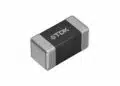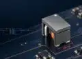



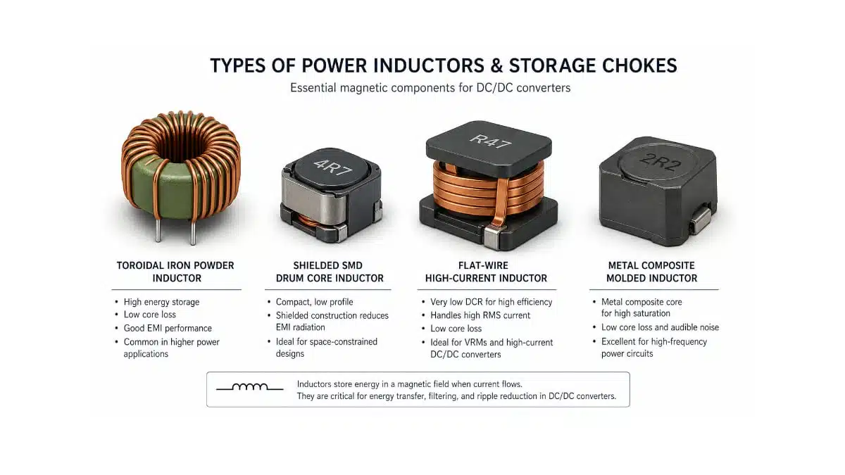
Switched-mode power supplies are becoming ever more widespread. The semiconductor manufacturers have made their contribution, offering a wide range these integrated circuits with simplified circuit design. Care must be taken in the selection of the appropriate power inductor storage choke to fully utilize the advantages of switching regulators.
In this article the terms power inductor and storage choke are used almost interchangeably.
In the context of switched‑mode power supplies they both denote inductors that primarily store energy in their magnetic field and control current ripple in the power path. “Storage choke” emphasises the energy‑buffering role in series with the load or switching node, while “power inductor” is the more general term used in datasheets and catalogues for inductors designed for higher currents and switching applications.
| Term | Typical usage in this article | Main emphasis |
|---|---|---|
| Storage choke | Inductor in the energy‑storing path of a SMPS (e.g. buck, boost, SEPIC) | Energy buffering and current ripple control in switching converters |
| Power inductor | General catalogue term for inductors used in power electronics | Current rating, losses, core technology and package for switching and DC/DC applications |
| Line / EMI suppression choke | Choke placed in series with supply lines, often on toroidal or common‑mode cores | Impedance to differential‑ or common‑mode noise for EMC compliance, not primarily energy storage |
Key Takeaways
- A power inductor is selected from the converter topology, switching frequency, ripple-current target, peak current, RMS current, thermal environment and EMC requirements—not from nominal inductance alone.
- Use the minimum inductance available at maximum DC bias, maximum operating temperature and worst-case production tolerance when assessing converter ripple, stability and peak current.
- Do not compare saturation-current values between manufacturers without checking the stated inductance-drop criterion, test temperature and measurement conditions. The complete inductance-versus-DC-bias curve is more informative.
- DCR determines DC copper loss, but winding AC resistance and core loss can dominate as switching frequency and ripple frequency increase.
- Ferrite, iron powder, alloy powder and moulded metal-composite cores each involve trade-offs among saturation behaviour, AC loss, size, temperature stability, cost and mechanical robustness.
- Validate the chosen inductor in the finished converter, including efficiency, temperature rise, startup, overload, transient response, audible noise and conducted/radiated EMI.
Design principle: Treat the power inductor as an electromagnetic, thermal and mechanical part of the complete power stage. A catalogue inductance value and a single current rating are only the starting point of selection.
Power Inductor Calculations
The selection of cores and windings of storage chokes are optimized for use in switching converters and DC-DC converters.
Power-converter IC manufacturers publish reference designs, design tools and layout recommendations that can help establish starting values for inductance, ripple current and current rating. These recommendations should be checked against the final operating conditions, magnetic tolerances and thermal environment of the finished design.
Toroidal Core Types
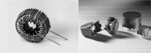
Toroidal storage chokes are ideal from the EMC perspective: The magnetic field lines mainly pass through the core. The stray field and associated coupling in neighboring conductor tracks or components remain small.
In the field of switching converters, storage chokes serve to buffer electrical energy and, at the same time, to smooth the output current. The energy stored in the core in this process is:
energy stored in storage choke inductor eq. 1.
Powder cores are made from electrically insulated magnetic particles. The insulation increases electrical resistivity and creates a distributed air-gap structure throughout the magnetic path. This structure supports energy storage under DC bias and helps limit eddy-current loss compared with an equivalent solid-metal core. Core loss nevertheless depends strongly on the selected powder alloy, particle size, binder system, switching frequency, flux-density swing and temperature.
The reduced effective permeability of a distributed-gap powder core requires more winding turns for a given inductance, but it can improve DC-bias tolerance and energy-storage capability. Whether total loss is lower than a ferrite alternative depends on the application operating point and must be established from component-specific core-loss, AC-loss and thermal data.
Data book specifications
Open-circuit inductance L0:
If the inductor is operated without DC premagnetization or with only a small AC current, the open-circuit inductance L0 results.This value may be measured with sufficiently sensitive inductance measuring equipment for small AC voltages e.g. 0.1–0.5 V and a fixed measuring frequency between 1 kHz and 100 kHz, depending on the inductance value.
Inductance rating LN:
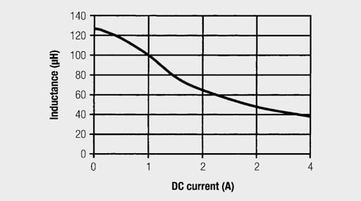
In addition to the small AC voltage amplitude, the specified DC current is superimposed and the resulting inductance measured.
Current rating IN:
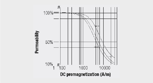
The DC current, for which the inductance and wire thickness are specified and whose specifications are optimized. As shown in graph on Figure 2., inductance only saturates with a much larger current.
DC resistance DCR:
The winding resistance value is measured with an ohmmeter at an ambient temperature of +25 °C.The test current for resistance measurement is a small DC current, which does not lead to a significant temperature increase in the wire. As values in the milliohm range are measured here, a 4-wire measurement must be made to minimize measurement errors.
Magnetic field energy E:
The energy, for which the core data and windings of the coil is optimized. This is specified in microjoules.The following simple and practically proven formulae can be used for dimensioning a storage choke. A brief extract from the extensive core material program and the following table should provide an overview of the choke dimensioning process. Depending on the application, further specifications from the core material data spectrum may be necessary.
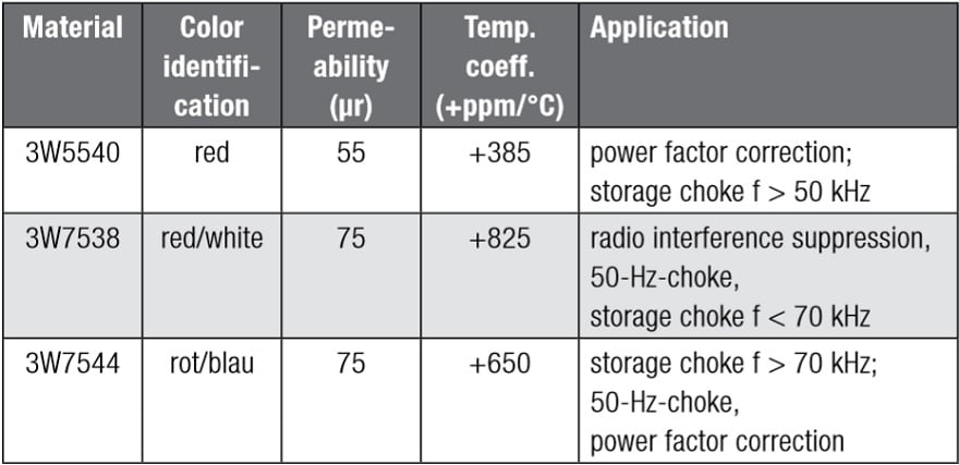
Iron core material data:
The table 1 shows an overview of the most commonly used materials and their applications.
Operating temperature:
The operating temperature of the iron powder core may be from –55 °C to +125 °C. Prolonged core operation above +75 °C however results in increased losses.
Insulation voltage:
The protective coating of the toroidal core uniquely identifies the core material and serves to protect against environmental effects and provides electrical isolation from the windings. Epoxy resin coatings are used and an insulation dielectric strength of 500 VDC is achieved as standard. Higher insulation voltages can also be offered.
AL value: For every size of core an AL value is specified to simply calculate the winding turns for the required choke; the tolerance is ±10%.
The standard means of measuring the AL value is at B = 1 mT and f = 10 kHz.
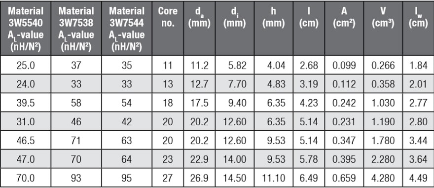
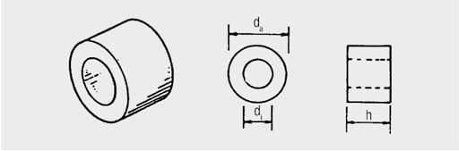
- da = outer diameter
- di = inner diameter
- h = height
- l = effective magnetic length
- A = effective magnetic cross-sectional area
- V = effective magnetic volume l
- W = winding wire length for 1 turn

Inductor Sizing From Converter Topology
The required inductance is determined by the converter topology, voltage range, switching frequency and permitted ripple current. The equations below apply to idealized continuous-conduction-mode operation and provide a starting point only. Semiconductor voltage drops, dead time, control strategy, minimum on/off time, magnetic tolerances and transient requirements must be included in the final design.
Buck converter
For a non-isolated buck converter, the highest ripple current usually occurs at the combination of input voltage, output voltage and switching frequency that produces the largest inductor voltage-time product. Under ideal steady-state conditions:
A ripple-current target of approximately 20% to 40% of maximum output current is often used as an initial compromise between inductor size, peak current, output-voltage ripple and transient response. The optimum value is application-specific; low-ripple designs generally need more inductance, while high-ripple designs can reduce inductance but increase RMS losses, peak switch current and output-capacitor stress.
Boost converter
In a boost converter, inductor current is the input current and can be substantially higher than output current. At maximum load, the inductor must be designed for the highest expected input current, including efficiency loss and transient margin.
For boost converters, the highest peak inductor current frequently occurs at minimum input voltage, maximum output power and maximum duty cycle. This operating corner should be used to check saturation margin and copper loss.
Continuous and discontinuous conduction
In continuous-conduction mode (CCM), the inductor current does not fall to zero within a switching cycle. CCM normally gives lower peak current and lower ripple at a given power level, but it requires sufficient inductance. In discontinuous-conduction mode (DCM), the current falls to zero each cycle; peak current, RMS current and EMI can rise significantly, while control behaviour changes.
Modern regulators may intentionally enter DCM, pulse-frequency modulation, burst mode or diode-emulation mode at light load to improve efficiency. These modes can alter inductor ripple, audible-noise behaviour and output-voltage ripple. The inductor should therefore be checked at full load, light load, startup and fast load transitions—not only at nominal steady-state conditions.
Selection checkpoint: Calculate DC, RMS and peak current separately. The RMS current drives copper loss, the peak current determines saturation margin, and the minimum inductance under bias determines current ripple and converter dynamics.
Storage Choke Design Example
The following demonstrates how a storage choke can be calculated for a switching converter application:
Example: switching converter (step-down controller – storage choke)
Requirements:
Inductance rating LN = 100 µH Current rating (DC) IN = 1 A Peak current through the inductance Imax = 1.5 A Ripple current = 20% of Imax = 0.3 A (see Chapter III/Applications) Switching frequency f = 52 kHz
A maximum AC flux density BAC = 0.05 T is recommended for iron powder cores (to ensure low core losses). Also the inductance should be selected so the ripple current does not exceed 20%–30% of the maximum current.
Step 1 : Choice of the core material and the necessary core volume (V). As the switching frequency is just 50 kHz, we firstly select the material 3W7538 with µr = 75.

Selected core: 3W7538, as switching frequency < 70 kHz; core no. 13 da = 12.7 mm; di = 7.7 mm; h = 4.83 mm
Magnetic data: l = 3.19 cm; A = 0.112 cm2; V = 0.358 cm3 AL value: 33 nH/N2
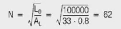
Step 2: Required winding turns

- L in nH
- AL value in nH/N2
The final number of winding turns must be increased as a result of current-dependent permeability. The correction factor for the AL value is determined from the “effective permeability against DC premagnetization” graph (see Figure 3.).
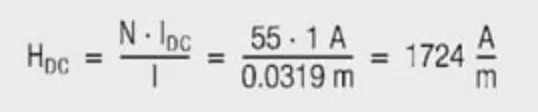
At H = 1724 A/m on the graph in Figure 3. → Effective permeability with DC premagnetization = 80% of the initial permeability.
To be certain that the full inductance rating of 100µH exists with a DC current of 1A, the final number of winding turns is calculated as:
Step 3: Determination of the DC resistance
The wire diameter can be ascertained from the relevant wire tables for the required current of 1A, e.g. AWG 22 (d = 0.6 mm). This limits the self-heating of the wire to less than +10°C.
The DC resistance of the windings is given by:

Step 4: Check for max. AC field flux density

- Inductance rating L in H
- Ripple current ΔI in A
- Core cross-sectional area A in cm2
- Winding turns N
- Peak voltage of the choke Us in V (during “t”)
- Duration of peak voltage t in s
Step 5: Calculation of core losses
The losses in the core material may be calculated from the following formula:

- Frequency f in Hz
- AC field flux density B in mT
- Core losses PC in mW/cm3
For our examples this leads to:
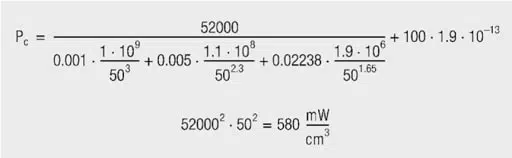
The total core losses of the selected core are:

The losses in the windings equal:

The total losses of the storage choke are low at around 370mW and the choke calculated is well suited for the application.
High-Current Power-Inductor Families
SMD NiZn Ferrite Power Inductors
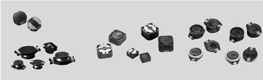
SMD power inductors using NiZn ferrite cores are available for switching converters from several hundred kilohertz into the MHz range. Their practical frequency limit is determined by the specific core material, AC flux-density swing, DC bias, winding losses, package construction and permitted temperature rise. Always use the loss, inductance-versus-current and thermal data for the selected component rather than applying a single frequency limit to all NiZn ferrite inductors.
There are a multitude of construction types available for the different types of application:
- Magnetically shielded series
- Unshielded versions series
Data book specifications
Inductance L: Different measurement conditions apply for the different construction series. The inductance is stated at a certain test frequency and measurement voltage (see data sheet).
Current rating IN: The current rating of the inductor is specified as the DC current at which inductor exceeds the permitted tolerance limits (DL) or the self-generated heating (DT) exceeds a certain limit. The smaller of the currents defined by the two conditions is termed the current rating of the inductor. This is however not the saturation current, which is higher than the current rating.
DC resistance DCR: The winding resistance value is measured with an ohmmeter at an ambient temperature of +20 °C. The test current for resistance measurement is a small DC current, which does not lead to a significant temperature increase in the wire. As values in the milliohm range are measured here, a 4-wire measurement must be made to minimize measurement errors.
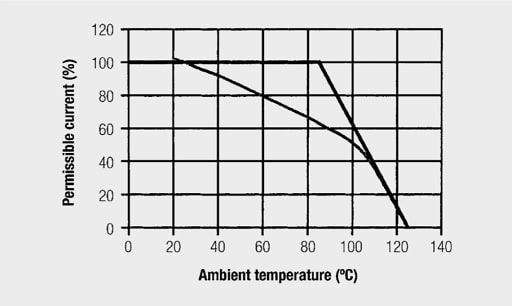
Operating temperature: The ambient temperature when operating the SMD NiZn series of storage chokes at full current rating load should generally range from –40 °C to +85 °C. The self-heating of the component must be taken into account at higher ambient temperatures in order that the permissible solder joint temperature is not exceeded or the wire insulation damaged. The wire used can withstand a temperature of up to +150 °C. The ferrite core itself may be used over a far greater temperature range (approx. –50 °C to +250 °C [Curie temperature]). However, in this case, the tolerance limits of the inductor may be exceeded due to the temperature dependence of permeability.
Operating temperature = ambient temperature + self-heating < +125 ºC
The above curve on Figure 5. assumes that self-heating is permissible up to a maximum temperature sum (component + ambient temperature) of +125 °C. The current must be reduced above an ambient temperature of +85 °C. The curve below is intended for critical applications, in which the coil itself should only generate a small amount of self-heating.
Insulation resistance: The insulation resistance between windings and coil core is more than 100 MΩ for a test voltage of 500 VDC<sub>DC</sub>.
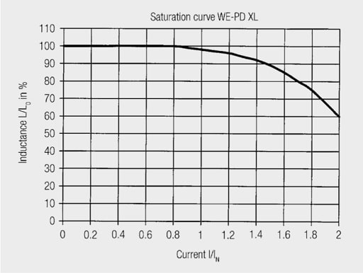
Saturation current Isat: The saturation current is the DC current at which the zero current inductance is reduced by a certain percentage.
The percentage of inductance decrease is however not standardised and can be defined differently for each package type. In datasheets – and especially when comparing data from different manufacturers – very close attention must be paid to the definition point. A printout of the measurement curve “Inductance versus DC premagnetization” is better still. Here the user can, for example, check in detail how the inductor behaves in the case of overload or at the moment it switches on. An example for a standardised curve is shown in Figure 6.
How to interpret current ratings
Power-inductor datasheets commonly list more than one current value. These values are useful only when their definition, test conditions and temperature limit are understood. A current labelled Isat may correspond to a specified reduction of inductance—often 10%, 20% or 30%—rather than to a safe continuous operating limit. A current labelled Irms, Irated or Iheat normally relates to a permitted temperature rise under defined PCB and ambient conditions.
| Parameter | What it indicates | How to use it in design |
|---|---|---|
| Nominal inductance, L0 | Inductance at the stated small-signal test frequency, AC level and usually near-zero DC bias | Use as a reference only; do not assume it remains available at operating current. |
| Inductance at bias | Actual inductance with specified DC current and sometimes specified temperature | Use the minimum value at worst-case current and temperature for ripple and control-loop calculations. |
| Saturation current, Isat | Current at a manufacturer-defined inductance reduction | Check the percentage drop and temperature. Preserve margin for startup, transient and fault current. |
| Rated or thermal current, Irms | Current producing a defined temperature rise under stated mounting conditions | Recalculate or validate for the actual PCB copper area, airflow, enclosure and neighbouring heat sources. |
| DCR | DC winding resistance, normally measured at 20 °C or 25 °C | Use the maximum specified value and correct for winding temperature when estimating copper loss. |
| AC resistance or impedance data | Frequency-dependent winding and parasitic behaviour | Important in high-ripple and MHz-range converters; use when available rather than assuming DCR is the total winding resistance. |
Practical rule: Select against the worst case, not the typical curve. Include inductance tolerance, DC-bias reduction, component temperature, maximum input voltage, startup, output short-circuit behaviour and transient current demand. Where the controller has cycle-by-cycle current limiting, verify that the inductor does not enter severe saturation before protection responds.
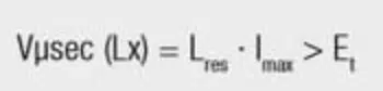
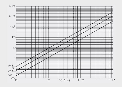
Volt-µsec product: As a result of their effective magnetic area Aeff, storage chokes can only be driven to a maximum value – the so-called Volt-µsec product. The following calculation rule applies for the step-down controller to determine the necessary Vµsec product of storage chokes:
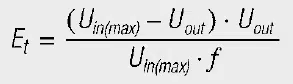
- Et = V-µsec
- Uin(max) the maximum input voltage in Volts
- Uout the output voltage of the controller
- f the switching frequency in Hz.
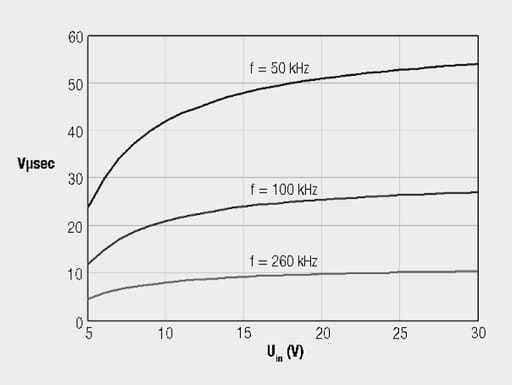
With increasing switching frequency, the necessary Vµsec product of the storage choke becomes lower; however, with increasing input voltage it becomes higher. This relationship is again illustrated in Figure 2.48 below.
Practical tips:
For some types in the SMD NiZn SMD chokes manufacturers also provide Vµsec specification in their datasheets. If this information is missing, it can be read off from the measurement curve “Inductance versus DC current premagnetization”. Here you locate the inductance plateau where you read off the associated current and residual inductance values and calculate the Vµsec product as follows:
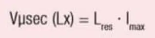
- Lres in µH
- Imax in A.
Ferrite storage chokes
Many ferrite-based power inductors exhibit a relatively sharp reduction of inductance once their usable DC-bias range is exceeded. This is often described as hard saturation. The onset and steepness of this reduction depend on core material, effective air gap, winding turns, temperature and package construction. Designers should use the component-specific inductance-versus-current curve and maintain margin between the worst-case peak current and the region of rapid inductance collapse.

Powdered-iron, alloy-powder and many moulded metal-composite cores have a distributed air-gap structure. Their inductance commonly decreases more gradually with DC bias than that of a comparable hard-saturating ferrite design; this behaviour is often described as soft saturation. The actual curve remains material- and component-specific, so the minimum inductance at operating current and temperature must still be verified.
When to use NiZn SMD chokes versus iron powder
In practice, SMD NiZn ferrite storage chokes are particularly well suited for:
- Low to medium current DC/DC converters with switching frequencies from a few hundred kHz up to several MHz.
- Space‑constrained designs where a low profile, magnetically shielded SMD footprint is more important than absolute energy storage.
- Noise‑sensitive environments (e.g. point‑of‑load regulators on digital boards) where reduced stray field is critical for EMC and signal integrity.
Toroidal iron powder storage chokes are typically preferred when:
- Large energy storage is needed at relatively modest switching frequencies (tens of kHz to low hundreds of kHz).
- The design benefits from soft saturation behaviour and gradual inductance reduction with DC bias.
- Through‑hole mounting, high current capability and very low external field are acceptable or advantageous, for example in industrial power stages or EMI suppression.
This helps to frame the detailed NiZn and iron powder characteristics in terms of concrete converter design choices.
NiZn storage choke core material parameters
The NiZn (WE-PD) core material parameters are described by the following power loss formula:

The corresponding curve is shown in Figure 8.
Power Loss and Temperature Increase in the Component
Now the power loss can be approximately determined, the question arises of the temperature rise of the component in operation. Measurement curves can be generated for the rise in temperature of the components with DC currents. Here the questions are to be resolved:
How was the component measured?
- mounted on a PCB with a lot of copper (= cooling element!) OR
- only the component via a thin and poor heat-conducting connection
After what time was the temperature read off from the component (thermal time constant !)
The following approximation formulas can be useful in the design phase; however they do not obviate measurement under real operating conditions. Determination of total power loss in the storage choke:
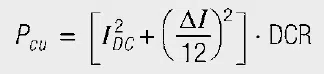
a) Copper losses:
b) Core material losses from empirical formulas
This results in the total power loss (without further losses such as the skin effect etc. …):

Temperature increase in the component (large surface)
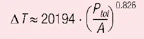
- Ptot in (W)
- surface area A in (mm2)
AC Loss, Core Loss and Thermal Design
A DCR-only calculation is adequate only when the ripple-current frequency is low and the winding AC resistance remains close to its DC value. In modern high-frequency converters, the inductor loss budget must include temperature-dependent DC copper loss, AC winding loss, core loss and any additional loss caused by fringing fields, terminals or eddy currents in nearby conductive structures.
Copper loss
DC winding loss can be estimated from the RMS inductor current and winding resistance at operating temperature:
Copper resistance rises by approximately 0.393% per °C near room temperature. A component specified at 2 mΩ at 25 °C therefore has materially higher DC loss when its winding operates at 100 °C. Use maximum DCR, not a typical value, for worst-case thermal estimation.
At higher switching frequencies, skin effect and proximity effect increase the effective winding resistance. The AC component of ripple current can then produce loss that is not predicted by DCR. Flat-wire and foil conductors can improve copper utilization, but their advantage depends on conductor thickness, current distribution, winding geometry, layer arrangement and frequency. Use manufacturer loss data or AC-resistance models where available.
Core loss
Core loss depends mainly on flux-density swing, switching frequency, waveform, temperature and DC bias. Material data are often represented by a Steinmetz-type relationship:
The coefficients k, α and β are material-specific and valid only over the stated frequency, flux-density and temperature range. Converter waveforms are not sinusoidal, so a simple sinusoidal-loss curve may not accurately predict loss under rectangular voltage excitation. When supplied by the manufacturer, use loss-versus-frequency and flux-density curves, loss maps, or models intended for non-sinusoidal waveforms.
System thermal validation
- Measure temperature rise on the actual PCB, because copper area, via stitching, board thickness, airflow, enclosure and neighbouring heat sources strongly affect the result.
- Allow the inductor to reach thermal steady state; the thermal time constant can be minutes rather than seconds.
- Use a thermocouple or a calibrated infrared method with appropriate emissivity treatment. Shiny terminals and dark mould compounds can otherwise produce misleading infrared readings.
- Check the hottest relevant point: winding, terminal, core or moulded body may not have the same temperature.
- Repeat the test at maximum ambient temperature, maximum load, worst-case input voltage and the highest expected switching frequency.
Important: A low DCR does not automatically mean a low-loss inductor. At high frequency, core loss and AC winding loss may become the dominant contributors to temperature rise.
Coupled Power Inductors With NiZn Ferrite Cores
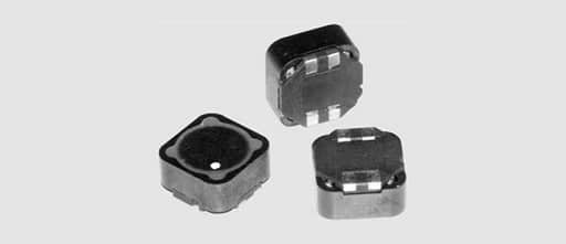
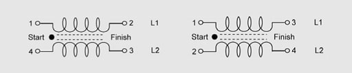
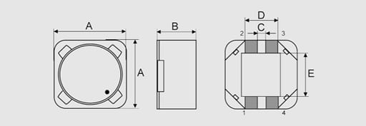
NiZn power ferrite core double chokes (Figure 9.) with two separate windings expand the standard spectrum of storage chokes with more features.
Features:
Two separate windings on a common ferrite core
- Available in a 1 : 1 winding (standard), but also in other winding ratios (customer-specific)
- Bifilar winding for minimal stray inductance / high coupling factor • (k ~ 0.985 … 0.990) or separate layer winding with increased leakage inductance
- Operating voltage up to 80VDC
- Isolation voltage 100VDC max
Applications:
- SEPIC switching controllers (functional principle – see Chapter III/7.4)
- CUK switching controller (switching controller with negative output voltage)
- Switching controllers with second, unregulated output voltage (auxiliary voltage)
Operating temperature:
The ambient temperature of double choke under full rated current load is usually between –40 °C and +85 °C. The self-heating of the component must be taken into account at higher ambient temperatures in order that the permissible solder joint temperature is not exceeded or the wire insulation damaged.
The wire used can withstand a temperature of up to +150 °C. The ferrite core itself may be used over a far greater temperature range (approx. –50 °C to +250 °C [Curie temperature]). However, in this case, the inductance tolerance limits may be exceeded due to the temperature dependence of permeability.
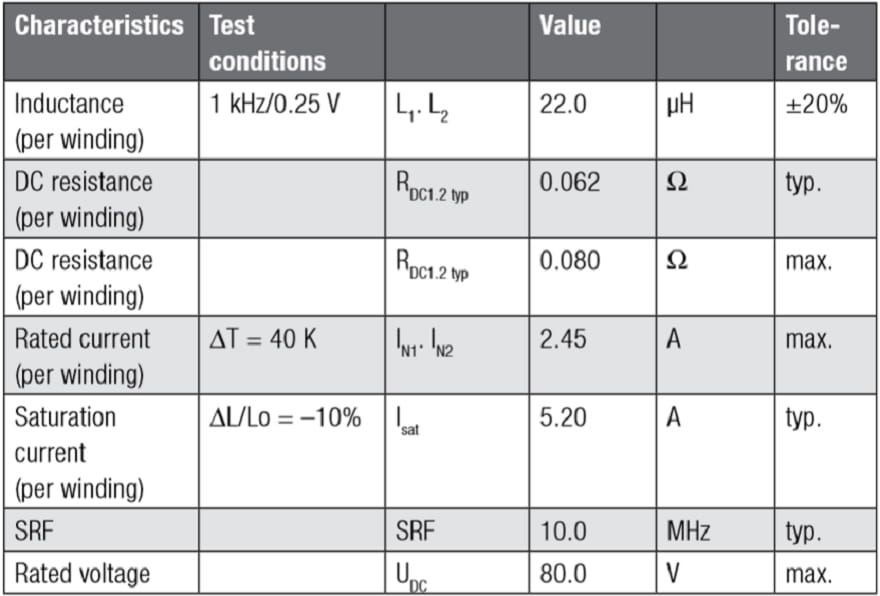
Electrical characteristics
Rated current: The self-heating for the pair of windings passing maximum current should not sum to more than +40°C. This is a conservative number, datasheet specification may differ per type and manufacturer.
Rated current is determined for each winding, which passes current on its own, leading to a temperature increase of up to +20 °C and is specified as IN1 and IN2 respectively. If both windings pass their rated current at the same time, this leads to self-heating totaling +40 °C.
DC resistance: Correspondingly, the specification for the winding resistance of the two individual windings is found from individual measurements. Attention: Please compare the datasheet specifications carefully – often the parallel configuration of the two windings is found in the literature as rated current / DC resistance, which suggests a higher rated current and lower DC resistance. In practice this is of course, not the application for this series of chokes!
Saturation current: In the case of the double choke with the same inductance, it is sufficient if just one of the windings carries the saturation current. The second winding is inevitably reduced in its inductance. The value is identical for the same inductance; the saturation current per winding is specified for dissimilar inductance values.
TPC “Tiny Power Choke“ SMD storage chokes
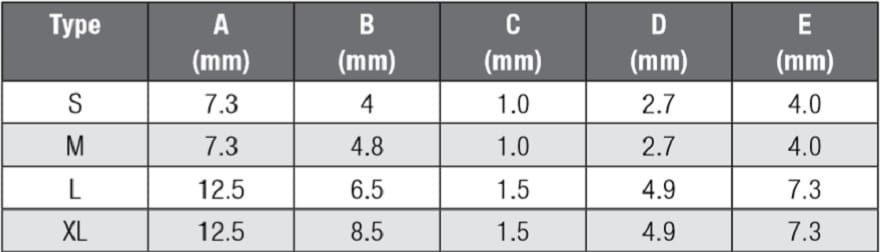
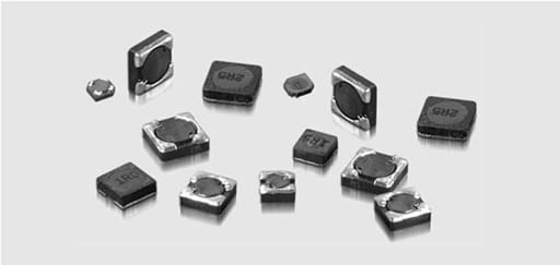
TPC “Tiny Power Choke“ of storage chokes (Figure 10.) is usually for applications for which the packing density and the package height is important. This design enable to produce the smallest wire-wound inductors in dimensions such as 2.8 x 2.8 x 1.0 mm.
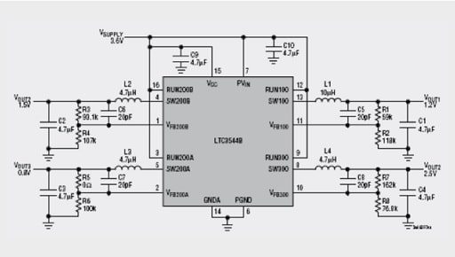
These chokes are mostly used for switching controllers that have several outputs integrated in one IC, e.g. LTC3544B. (Figure 11.) This IC has 4 outputs at which different voltages, output currents and switching frequencies are adjustable.
The core material used is typically NiZn and is therefore suitable for switching frequencies up to 10 MHz. The saturation current is defined as a –35% inductance drop in relation to the zero current inductance, which is usually typical for inductance in this small package. Magnetically shielded miniature inductors are useful in compact designs where coupling into nearby analogue, RF, sensing or communication circuitry must be controlled. Typical applications include portable electronics, embedded systems, cameras, communication modules and densely populated digital boards.
High-Current SMD Power Inductors
Laptop computers and motherboards of modern computers are equipped with processors, whose clock frequencies may be 1 GHz or more. Processor manufacturers rely on low supply voltages in order to maintain losses in integrated circuits within tolerable limits and to attain the required switching speeds. These lie between 1 … 3.3 Volts depending on the processor generation.
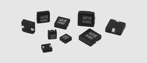
Modern processors, GPUs, FPGAs and AI accelerators operate from low-voltage rails that can demand hundreds of amperes at the load. Multiphase buck converters distribute this demand among several interleaved power stages. Each phase requires an inductor with tightly controlled inductance under DC bias, low total loss, predictable thermal behaviour and low stray-field coupling to neighbouring phases and sensitive control circuitry.
The core material used for high current inductors may require high-purity alloy of various types of iron powders, which shows significantly lower core losses than conventional iron powder cores.
Thermal aging: Thermal aging can lead to the destruction of the organic binder used, especially at high operating temperatures with standard iron powder material. A thermal avalanche effect can consequently occur, which may finally destroy the core material. For standard iron powder materials and those not thermally treated for reasons of their production process, the rule of thumb applies that the maximum temperature of +125 °C measured at the component should not be exceeded for a prolonged period. Nevertheless, modern materials with practically no thermal aging are now also available by leading manufacturers.
The core material of high current inductors can withstand high temperatures up to +200°C or even higher.
Flat-Conductor High-Current Inductors
High-current power inductors may use rectangular or flat conductors instead of round wire. A well-designed flat-conductor winding (Figure 13.) can improve use of the winding window, reduce DC resistance and shorten high-current interconnect paths. Its AC-loss performance must still be evaluated for the intended switching frequency and ripple-current spectrum, because skin effect, proximity effect, conductor thickness, layer count and local magnetic-field distribution influence the effective AC resistance.
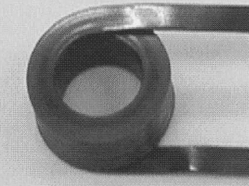
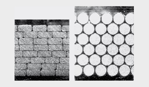
Flat wire windings offer the following advantages:
Large wire surface – thus low high-frequency losses (skin effect)
- Low winding capacity – hence high self-resonant frequency
- Low DC resistance – thus low self-heating at high prolonged currents
- High packing density and therefore smaller component size than comparable chokes with round wire (Figure 2.57)
- Maximum operating temperature determined by the complete component specification, including the core, winding insulation, moulding compound, terminals, solder-joint limit and specified derating conditions.
Through the combination of low-loss core material and flat wire windings inside the core, achievable performance of SMD high-current inductors can be:
- Small SMD component size such as 6.6 x 7.3 mm2, 10.5 x 10.0 mm2 or 13.5 x 12.8 mm2 with a height of 3.4 mm to max. 4.9 mm.
- Open-circuit inductance is specified at the test frequency and AC excitation level stated in the component datasheet. These conditions differ by product family and should be recorded whenever parts from different suppliers are compared.
- Inductance rating LN at current rating IN and self-heating < +50 °C
- Min. inductance at max. current Imax and self-heating < +100 °C
- Min. DC winding resistance DCRmax at Ta = +25 °C
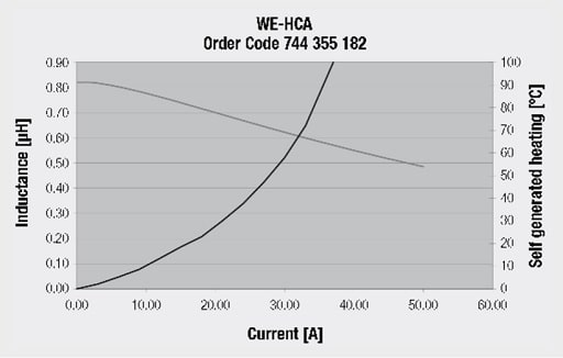
Figure 15. shows the typical behavior of SMD high-current inductor 0.82 µH choke 13.2 x 12.8 x 6.2 mm.
The component has an inductance of 0.65 µH at the specified rated current of 27 A and demonstrates typical self-heating of +50 °C. The inductance is very stable under current load; the limiting factor is the self-heating of the component. Even at a current load of 50 A the inductance does not drop more than 30% from the open-circuit inductance. The self-heating is well over +100 °C, however.
Flat wire, low core loss inductors represents a highly dynamic and robust types of storage chokes, especially suited for use in high-current switching converters and multiphase or polyphase converters. Additional application areas are in high-current interference suppression chokes and as a replacement for rod core chokes.
Power-Inductor Family Comparison
The following overview summarises typical characteristics of the main storage choke families discussed in this article.
| Inductor family | Typical frequency range | Saturation behaviour | DC bias / inductance trend | EMI and stray field | Mechanical robustness | Typical applications |
|---|---|---|---|---|---|---|
| Toroidal iron powder storage choke | ~20 kHz – 300 kHz | Soft saturation | Gradual inductance decrease with DC current, high usable energy | Very low stray field due to closed magnetic path | Good; through‑hole mounting, epoxy‑coated core | Energy storage in offline SMPS, PFC chokes, high‑current DC filtering, radio interference suppression |
| SMD NiZn ferrite storage choke (shielded / unshielded) | ~100 kHz – 10 MHz | Hard saturation | Inductance relatively constant up to a defined DC bias, then sharp drop | Shielded versions offer low stray field; unshielded versions higher EMI but lower cost | Moderate; SMD package, sensitive to shock compared to composites | General‑purpose DC/DC converters, POL regulators, RF‑friendly power rails |
| NiZn double chokes (two windings on common core) | ~100 kHz – few MHz | Ferrite hard saturation on overloaded winding | Strong coupling between windings; saturation of one winding affects the other | Shielded constructions offer good EMI, suitable for compact layouts | Similar to SMD NiZn storage chokes | SEPIC and Ćuk converters, auxiliary supply rails, multi‑output converters |
| Tiny Power Choke (TPC) SMD | ~1 MHz – 10 MHz | Hard saturation | Inductance drop dominated by small core and high current density | Shielded miniaturised packages reduce coupling into nearby traces | Mechanically modest but optimised for dense handheld / mobile layouts | Multi‑output low‑power DC/DCs in mobile and portable equipment, camera and RF modules |
| SMD high‑current, flat‑wire inductors | ~100 kHz – few MHz | Soft to moderate saturation, depending on core alloy | Very stable inductance over a wide current range, low DCR | Typically shielded; designed to minimise both copper and core losses | High; robust construction, often with high thermal rating | Multiphase VRMs for CPUs/GPUs/AI accelerators, high‑current POLs, high‑efficiency server and telecom converters |
| Radio interference suppression toroidal chokes | ~25 kHz – 30 MHz (impedance role) | Soft saturation in normal operation region | Selected for impedance versus frequency rather than energy storage | Very low stray field; designed to present high impedance to differential‑mode noise | Good; toroidal, through‑hole, often potted | Differential‑mode EMI suppression at converter input/output, filters in industrial and automotive power lines |
| Metal composite power inductors | ~100 kHz – several MHz | Often gradual inductance reduction under DC bias | Commonly strong DC-bias tolerance due to distributed microscopic air gaps; evaluate the actual L-versus-DC-bias curve | Frequently low external field in moulded, shielded constructions; verify coupling on the assembled PCB | Construction- and qualification-specific; review vibration, shock, board-flex and terminal-strength data for the exact part | High-current automotive, industrial, server, telecom and point-of-load applications where compact size, current capability and controlled stray field are important |
PCB Layout, Magnetic Coupling and Audible Noise
PCB layout rules
- Minimize the hot loop formed by the switching devices, input ceramic capacitors and their return path. This loop is typically a stronger source of high-frequency EMI than the inductor alone.
- Keep sensitive feedback, compensation, current-sense, clock, RF and analogue traces away from the switch node and from the strongest external magnetic field around the inductor.
- Avoid placing copper planes or signal traces directly beneath an unshielded inductor unless the effect on eddy-current loss, coupling and EMI has been checked.
- Use short, wide copper connections for high-current inductors, but keep the power-stage current return path controlled and avoid creating large loop areas.
- For multiphase regulators, evaluate inductor placement and orientation as a system. Adjacent magnetic fields can couple and affect EMI, current sensing and thermal distribution.
Audible-noise mechanisms
Power inductors can generate audible noise through magnetostriction, movement of windings or core parts, terminal vibration and excitation of the PCB. The effect can be especially noticeable during startup, light-load burst operation, pulse skipping, fault recovery or load transients, even when the normal switching frequency is above the audible range.
Possible mitigation measures include selecting a mechanically robust moulded or bonded construction, avoiding control modes that produce audible-frequency energy where practical, improving PCB stiffness, reviewing mounting and terminal stress, and reducing excessive ripple current or core excitation. Always confirm the result on the finished assembly because the PCB and enclosure can amplify a component-level vibration.
Layout reminder: Shielded inductors reduce field coupling, but they do not compensate for a large switch-node loop or poor input-capacitor placement.
EMI Suppression Chokes
In contrast to the energy‑storing power inductors and storage chokes discussed so far, the “choke” in this section is used in the EMI sense, where the component is optimised for impedance to conducted noise rather than for bulk energy storage.
Radio interference suppression chokes use usually iron powder toroidal cores with a very low stray field. High current loading capacity is achieved through high saturation magnetization. The useable maximum upper frequency range of this component extends from a few MHz to approx. 30 MHz depending on the type.
The impedance-phase curve against frequency of a typical toroidal core choke is shown in Figures 16. and 17.
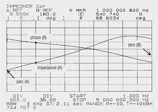
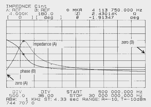
It may be seen from Figure 17. that the resonant frequency is at 4.1 MHz. Above 4.1 MHz the capacitive character of the choke predominates, at 30 MHz the impedance has fallen to approx. 200 Ω. The impedance is almost linear (Figure 16.) up to the resonant frequency of 4.1 MHz.
Due to the frequency dependence of complex permeability, calculations are only feasible in limited frequency bandwidths and sufficiently far (in the linear range) below the resonant frequency. Figure 18. shows the equivalent circuit of the choke in the 25 kHz to 1 MHz range, Figure 19. the equivalent circuit in the 1 MHz to 5 MHz range. The values were found using an impedance analyzer, calculating on the basis of the components’ equivalent circuit. Due to high non-linearity, the equivalent circuit can be simulated over a wide frequency range with just 3 components.
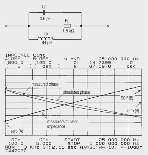
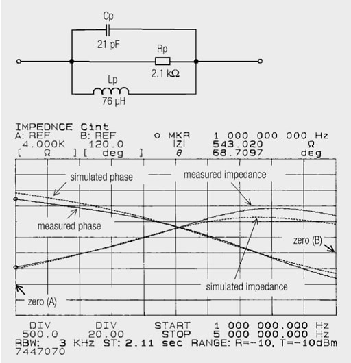
From the measurement curves impedance and phase an increase in eddy-current losses and a decrease in the complex permeability can be seen.
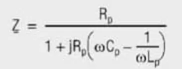
the impedance can be calculated as a function of frequency. The broken line in Figures 18. and 19. are the simulated curves with the values given by the equivalent circuits. It shows that without considering the complex permeability and its frequency dependence, the calculation can be performed with limited accuracy.
Practical tip:
Here another word on the saturation of the ferrite ring: The effective core cross-sectional area is inversely proportional to the saturation current and proportional to the impedance. This means that wherever possible, the larger core cross-section area should be chosen.
High‑frequency and wide‑bandgap trends
Higher switching frequencies can reduce the required inductance and magnetic volume, but they increase the importance of AC winding loss, core loss, parasitic capacitance, self-resonance and thermal management. These trade-offs are discussed further in the section Future Directions: Low-Loss, High-Density and Integrated Power Inductors.
Prototype Validation and Measurement
Datasheet values are measured under defined conditions that may not reproduce the electrical, thermal or mechanical environment of the final converter. Prototype validation should therefore confirm both the inductor characteristics and the behaviour of the complete power stage.
| Validation task | What to check | Practical note |
|---|---|---|
| Inductance and DC bias | Inductance across the expected DC-current range and, where possible, at elevated temperature | Use the minimum measured inductance for ripple and stability assessment. |
| DCR | Winding resistance and its temperature rise | Use a four-wire/Kelvin method because milliohm-level measurements are easily distorted by test leads and contacts. |
| Current waveform | Peak current, ripple current, startup current, overload behaviour and current-limit response | Use a correctly bandwidth-limited current probe or a validated current-sense method. |
| Temperature rise | Inductor body, terminals, adjacent capacitors and PCB hot spots at thermal equilibrium | Test with realistic airflow, enclosure and neighbouring heat sources. |
| Efficiency and loss | Converter efficiency across input voltage and load range | Correlate measured loss with DCR, core-loss and AC-loss estimates; investigate deviations. |
| EMI | Conducted and radiated emissions, switch-node ringing and magnetic coupling | Assess the assembled board. The inductor cannot be evaluated independently of layout and switching transitions. |
| Acoustic behaviour | Noise during light load, startup, transient response and protection events | Check the intended enclosure because mechanical resonances can amplify sound. |
For impedance and self-resonant-frequency work, use a suitable impedance analyzer or vector network analyzer with fixture compensation. For thermal work, allow sufficient settling time and document the PCB, copper area, airflow, ambient temperature and measurement position. This information is essential if results are to be compared between prototypes or used as a design baseline.
Future Directions in Power Inductors
The established selection principles described above — inductance under DC bias, saturation margin, DCR, AC loss, thermal behaviour and magnetic shielding — remain fundamental. However, the design priorities of power inductors are increasingly shaped by higher switching frequencies, higher current density and the need to fit more power into less PCB area and height.
Modern GaN- and SiC-based converters can operate from several hundred kilohertz into the MHz range. Raising switching frequency can reduce the required energy-storage inductance, but it also makes winding AC resistance, proximity effects, core loss, parasitic capacitance and thermal behaviour more critical. Inductor selection for these converters should therefore be based on loss-versus-frequency and temperature data, not on nominal inductance and DC current rating alone.
Lower RDC and reduced total loss
A central industry trend is the reduction of winding resistance and total DC loss while maintaining — or increasing — current capability. Since copper loss is approximately:
even a small reduction in DCR can have a substantial thermal benefit in high-current point-of-load converters. This is particularly important in CPU, GPU, FPGA and AI-accelerator voltage-regulator modules, where each phase may carry tens of amperes.
The main construction measures include:
- Flat-wire or rectangular-conductor windings, which use the available winding window more efficiently than round wire
- Short, wide terminal and clip interconnections that reduce resistive path length
- Optimised winding geometry to limit skin- and proximity-effect losses at high frequency
- Improved magnetic powders and nanocrystalline or alloy-based core materials with lower AC loss
Flat-wire inductors discussed earlier in this article remain highly relevant, but current designs increasingly combine such windings with moulded metal-composite cores and highly integrated terminal structures.
Moulded alloy and composite cores
Moulded metal-composite inductors are increasingly used in applications that demand high DC-bias capability, compact dimensions, controlled stray field and robust mechanical construction. They coexist with gapped ferrite, toroidal powder and other magnetic solutions, each of which remains appropriate in particular frequency, loss, cost, isolation and package-volume ranges.
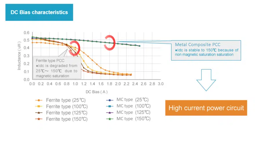
This behaviour offers a useful overload margin in high-current converters, although it does not eliminate the need to verify minimum inductance at peak current and worst-case temperature. The designer should still evaluate the complete L-versus-, the RMS current, core-loss curves and thermal derating.
New composite approaches are also targeting improved resistance to long-term temperature and voltage stress. Better binder systems, including polymer-based and inorganic material approaches, seek to improve thermal stability, reduce material degradation and enable use of more advanced magnetic powders.
Clip inductors for multiphase VRMs
Multiphase buck converters are essential wherever low-voltage loads demand very high current with fast transient response — notably processors, GPUs, AI accelerators, networking ASICs and data-centre power rails. In these designs, clip-based power inductors are becoming increasingly important.
A clip inductor replaces portions of the conventional wire connection with a formed metal conductor. This enables a low-resistance current path, compact winding geometry and improved repeatability in high-volume manufacture. Coupled, dual-coil or multi-coil implementations can also support multiphase architectures and transient-load-voltage-regulation concepts.
| Design feature | Design benefit | Typical target application |
|---|---|---|
| Flat wire or metal clip terminals | Reduced DCR and improved high-current capability | CPU, GPU and AI-accelerator VRMs |
| Moulded powder core | Soft saturation and stable inductance under DC bias | Multiphase POL converters |
| Coupled multi-coil construction | Improved transient response and current sharing potential | Advanced server and processor power stages |
| Compact, shielded package | Lower leakage flux and better PCB integration | Dense digital and telecom boards |
For these applications, inductor choice must be coordinated with the controller strategy, phase count, switching frequency, transient target and PCB thermal design. The inductor is no longer an isolated component choice; it is part of the complete power-stage optimisation.
Silicon-based and embedded inductors
A more emerging development is the fabrication of inductors using semiconductor and wafer-level processes. Silicon-based inductors can integrate copper conductors and magnetic films into ultra-thin structures, potentially allowing direct embedding, advanced package integration or chiplet-level power delivery.
Their principal attraction is not replacement of large discrete power inductors in high-power rails. Rather, they are relevant where profile, assembly integration and high-volume production matter most: compact mobile devices, wearables, IoT modules and highly integrated low-power converters.
At present, this technology is best viewed as complementary to conventional wound and moulded inductors:
| Technology | Principal advantage | Most suitable use |
|---|---|---|
| Wound ferrite or metal-composite inductor | High current and practical energy storage | Board-level DC/DC converters and VRMs |
| Flat-wire / clip inductor | Very low DCR and high power density | CPUs, GPUs, servers and automotive POLs |
| Wafer-level silicon inductor | Ultra-low profile and integration potential | Low-power embedded and package-level converters |
AI-assisted magnetic design
Digital simulation, optimisation algorithms and AI-assisted design tools are increasingly used to shorten magnetic-component development. They can accelerate optimisation of core geometry, conductor shape, powder composition, thermal paths and parasitics, while digital-twin methods can help predict loss and temperature under realistic electrical mission profiles.
For the circuit designer, this makes high-quality manufacturer models increasingly valuable. Where available, use loss models, thermal models, DC-bias curves and S-parameter or impedance data rather than relying solely on headline catalogue values. This is especially important at MHz-range switching frequencies, where parasitic effects can materially influence efficiency, ringing and EMI.
Practical selection implications
The future-oriented design rules for power inductors are therefore straightforward:
- Specify current correctly: Calculate DC, RMS, peak, start-up and transient current separately; do not use a single “current rating” as a complete selection criterion.
- Evaluate losses at operating conditions: Check DCR, AC winding loss and core loss at the actual switching frequency, ripple current and temperature.
- Use the DC-bias curve: Confirm sufficient inductance at maximum DC current and worst-case temperature, with margin for tolerances and transients.
- Treat thermal design as a system task: Account for copper area, airflow, component spacing, nearby heat sources and the actual PCB stack-up used for validation.
- Select the construction for the application: Use ferrite types for low-loss high-frequency operation where their saturation characteristics are acceptable; use metal-composite and moulded-powder types for strong DC-bias performance and robustness; consider flat-wire or clip designs when DCR and current density dominate.
- Validate EMI and mechanics: Confirm shielding, leakage field, vibration, shock, insulation and qualification requirements, especially in automotive, industrial and data-centre applications.
These developments do not replace the fundamental calculations in this article. They reinforce the importance of evaluating the inductor as an electro-magnetic, thermal and mechanical component within the complete converter rather than selecting it only by nominal inductance and catalogue current rating.
Moulded Metal-Composite Power Inductors
Moulded metal-composite power inductors use insulated magnetic-powder particles embedded in a binder and formed around the winding or conductor system. The distributed air-gap structure gives gradual inductance reduction with DC bias, often described as soft saturation. This can be advantageous in compact high-current designs because the inductance changes progressively rather than collapsing abruptly at a single current threshold.
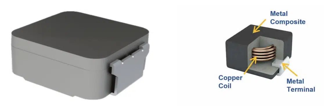
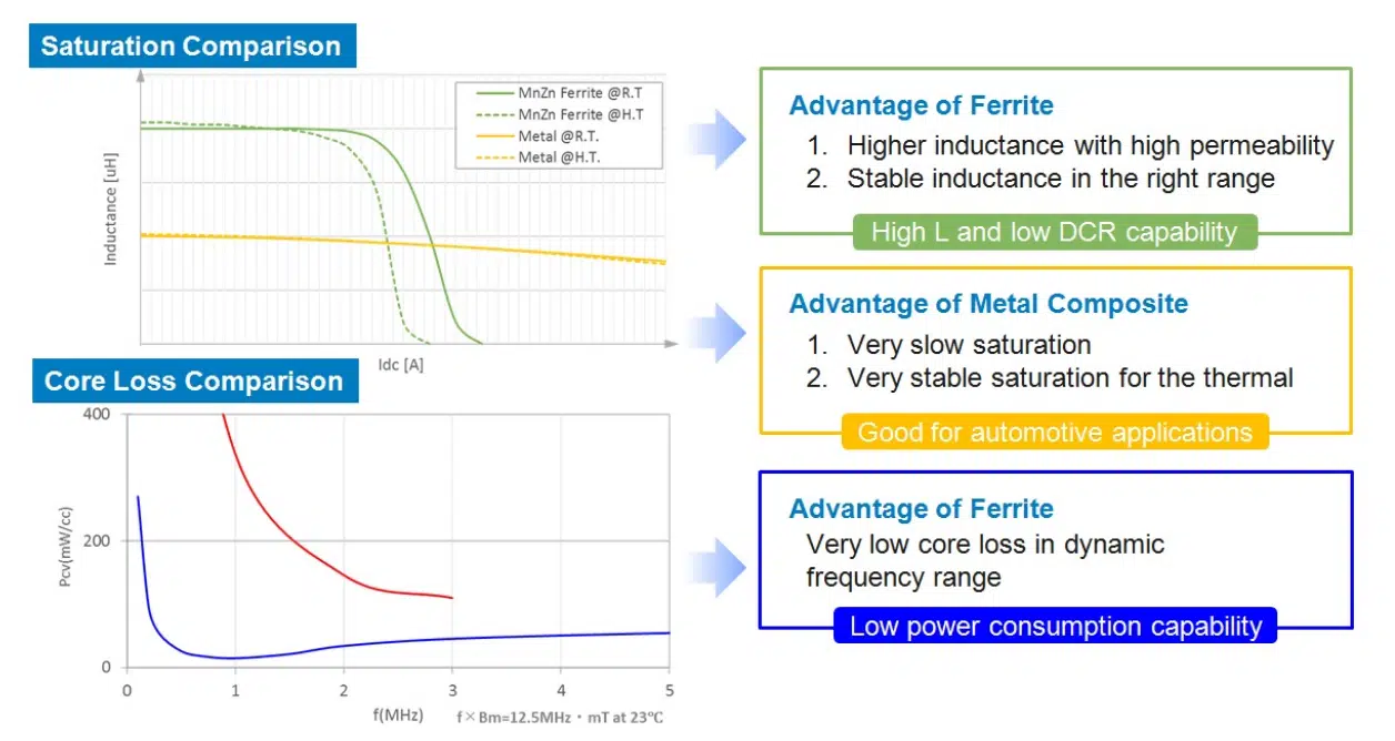
Metal-composite construction is not a universal replacement for ferrite. The correct choice depends on switching frequency, AC flux swing, required inductance, DC bias, loss target, operating temperature, package volume, height limit, qualification needs and cost. Ferrite can provide very low loss in suitable high-frequency, lower-flux applications, while moulded powder materials can offer attractive bias tolerance, compact shielding and mechanical integration in high-current power rails.
| Characteristic | Gapped ferrite construction | Moulded metal-composite construction | Design implication |
|---|---|---|---|
| Energy-storage mechanism | Usually a discrete or distributed effective air gap in a ferrite magnetic path | Distributed microscopic gaps between insulated powder particles | Both can store energy; compare inductance-versus-current curves at the required operating point. |
| Saturation behaviour | Often relatively abrupt beyond the usable bias range | Usually more gradual inductance reduction with increasing DC bias | Soft saturation is useful for overload tolerance but does not remove the need for peak-current margin. |
| Core-loss behaviour | Can be very favourable at suitable frequency, flux swing and temperature | Depends strongly on powder alloy, particle insulation, binder and frequency | Use product-specific loss curves; no material family is lowest loss under every condition. |
| Shielding and leakage field | Depends on core geometry and package; shielded versions can perform well | Often naturally well-contained in monolithic moulded packages | Verify actual magnetic-field coupling in the final PCB layout. |
| Mechanical construction | May use assembled core parts and winding structures | Typically monolithic body around the magnetic structure | Review product-specific shock, vibration, board-flex and terminal-strength data. |
| Typical applications | High-frequency DC/DC conversion, compact shielded inductors, general power supplies | High-current POL rails, automotive modules, industrial power stages and compact VRMs | Select from measured electrical and thermal performance rather than construction alone. |
Mechanical and environmental requirements
Mechanical robustness is determined by the individual component construction and qualification programme, not by core material alone. For automotive, industrial, aerospace or other mission-profile-driven applications, review the supplier’s evidence for temperature cycling, high-temperature storage, humidity, vibration, mechanical shock, solder-joint reliability, terminal strength and resistance to PCB flexure.
Where automotive qualification is required, verify the applicable AEC-Q200 status for the exact ordering code and ensure that the available test data match the actual mission profile. Qualification does not eliminate application-level validation: board resonance, mounting orientation, potting materials, connector loads and enclosure vibration can create stresses that are not represented by a single component test.
EMI and stray-field control
A moulded or shielded package can reduce external magnetic field, but it does not replace good power-stage layout. Keep the high-di/dt switching loop compact, locate the input ceramic capacitors close to the switching devices, and avoid routing sensitive feedback, current-sense, clock, RF or high-impedance analogue traces beneath or beside the inductor. When several inductors are used on one PCB, consider their orientation and spacing to minimize magnetic coupling.
Final conducted and radiated EMI performance depends on the entire converter: the switch-node voltage slew rate, ringing, capacitor placement, ground return path, PCB stack-up, enclosure and cable interfaces can be as important as the inductor construction itself.
Low EMI Noise
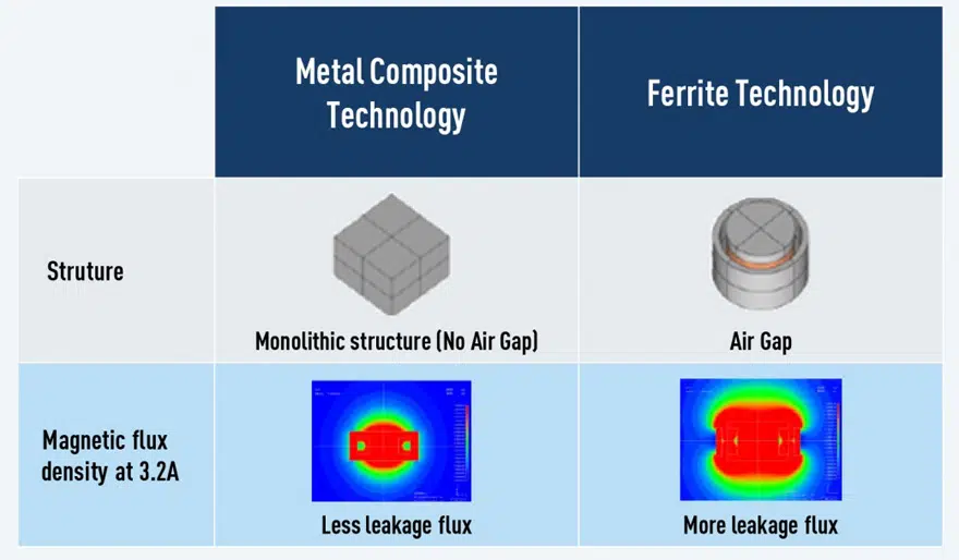
Also in terms of a lower leakage flux outside the power inductors, the point goes to the metal composite types: Their monolithic structure causes by far less leakage as the magnetic flux simply is concentrated inside the inductor housing. See figure 23.
Conclusion
Power inductors and storage chokes are critical energy-storage, current-shaping and thermal components in switching converters. Reliable selection requires more than matching nominal inductance and a catalogue current rating: the designer must evaluate inductance under DC bias, peak and RMS current, DCR, AC winding loss, core loss, temperature rise, magnetic-field containment and mechanical requirements at the actual operating conditions.
No single core material or package is optimal for every design. Gapped ferrite, iron-powder, alloy-powder, moulded metal-composite, toroidal and coupled-inductor solutions each provide different trade-offs in frequency capability, loss, saturation behaviour, size, EMI and cost. Final component selection should be confirmed through converter-level testing across the full input-voltage, load, temperature, startup, transient and EMI range.
Final design rule: Choose the inductor from its worst-case electrical, thermal and mechanical operating point—and validate it on the final PCB—not from nominal inductance alone.
References
inductor fundamentals and key electrical parameters
inductor core materials and magnetic-loss mechanisms
toroidal and current-compensated choke constructions
why power inductors use a ferrite core with an air gap
current sensing in high-current power-conversion systems
FAQ
A storage choke (power inductor) stores energy in its magnetic field during the on-time of the switch and releases it during the off-time. This energy buffering smooths the inductor current, limits ripple, and helps shape the output voltage and dynamic response of the converter.
Toroidal iron powder chokes are preferred for lower-frequency converters that need high energy storage, soft saturation, and very low stray field, typically in through-hole designs. SMD NiZn ferrite inductors are better for compact, higher-frequency DC/DC converters where shielded SMD packaging and tight EMI control are more important than maximum stored energy.
The inductance versus DC bias curve shows how the effective inductance decreases as DC current increases. This helps you verify that the inductor still provides sufficient inductance at the real operating current and that you are not driving it too close to hard saturation, especially for ferrite cores.
The Volt‑µsec rating limits how much voltage and on-time can be applied to an inductor before the core saturates. In buck converters, it relates directly to input voltage, output voltage, and switching frequency and must exceed the required V·µs to ensure reliable operation without core saturation.
Metal composite inductors are ideal when you need high current capability, excellent DC bias stability, low core losses, and robust mechanical performance, for example in automotive ECUs, industrial controllers, and multiphase VRMs. They typically allow smaller case sizes, higher vibration resistance, and more predictable inductance over temperature compared to many ferrite solutions.
Important parameters include nominal inductance and test conditions, DC resistance (DCR), current rating and its definition (temperature rise versus inductance drop), saturation or Isat curves, DC bias versus inductance curves, core loss behaviour, Volt‑µsec rating, operating temperature range, and any derating curves or AEC‑Q200 qualifications relevant to the application.
Consider moulded metal-composite inductors when strong DC-bias tolerance, compact shielding, gradual inductance reduction under overload, high current density or mechanical integration are major requirements. Ferrite remains a strong choice where its low-loss performance at the required frequency and flux swing, package availability and cost are favorable. Compare actual inductance-versus-current, loss-versus-frequency and thermal data for the candidate parts rather than selecting solely by material family.
Check nominal inductance and its test conditions, inductance tolerance, the inductance-versus-DC-bias curve, saturation-current definition, rated-current or temperature-rise definition, maximum DCR, operating-temperature range, thermal derating, core-loss or total-loss data, self-resonant frequency where relevant, insulation requirements, package dimensions and qualification status. For high-frequency converters, also look for AC-resistance, impedance or manufacturer loss-model information.
How to select a power inductor for a DC/DC converter
- Define converter topology and requirements
Identify whether you are using a buck, boost, buck‑boost, SEPIC, Ćuk or multiphase VRM topology. Specify input voltage range, output voltage, maximum load current, allowable inductor current ripple (for example 20–30% of peak current) and switching frequency.
- Calculate the target inductance and current ratings
Use the appropriate topology equations to derive the nominal inductance value from the chosen ripple and frequency. Determine peak, RMS and DC currents through the inductor under worst‑case operating conditions, including start‑up and transients.
- Choose a suitable core material family
Select a core material based on frequency, DC bias and efficiency targets: ferrite for hard‑saturating, low‑loss operation at higher frequencies, iron powder for soft saturation and high energy storage at lower frequencies, or metal composite for high current, soft saturation and robust temperature behaviour.
- Select construction and package type
Decide between toroidal, SMD drum, double choke, Tiny Power Choke, flat‑wire high‑current or metal composite constructions according to required current, available PCB area and height, cooling, soldering technology and EMI constraints. Consider whether you need shielded or unshielded versions.
- Check DC bias, Volt‑µsec and derating curves
From candidate datasheets, verify that the inductance versus DC bias curve remains within your tolerance at the operating current. Confirm that the inductor’s Volt‑µsec capability exceeds the required V·µs for your converter across the full input range, and review any temperature or current derating curves.
- Estimate core and copper losses
Use the core loss data (Steinmetz or tabulated curves) and the calculated AC flux density to estimate core losses, and combine them with I²R copper losses based on DCR and current waveform. Ensure total loss is compatible with your efficiency targets.
- Verify temperature rise and operating limits
Use manufacturer thermal data or simple surface‑area‑based approximations to estimate temperature rise at the calculated total losses. Check that the sum of ambient temperature and self‑heating stays within the specified operating range of the inductor and your overall thermal design limits.
- Validate against application‑specific constraints
Finally, confirm that the chosen inductor meets application‑specific requirements such as AEC‑Q200 qualification for automotive, mechanical shock and vibration limits, insulation voltage, and EMI performance in your filter or layout. Adjust the inductor family or size if needed and iterate the calculations.
Further Reading on Passive Components Blog:
The following articles provide additional background on magnetic-component technology and related design considerations:
- Why power inductors use a ferrite core with an air gap — explains energy storage, gap-related saturation margin and fringing-field considerations.
- Current-sense transformers: ferrite versus nanocrystalline cores for accurate current measurement — useful background for high-current converter measurement and magnetic-material trade-offs.
- Inductor fundamentals and key electrical parameters
- Inductor core materials and magnetic-loss mechanisms
For detailed step‑by‑step guidance on turning the concepts and formulas in this article into a concrete inductor choice for a given converter design, see also: Selection of the Storage Inductors for DC/DC Converters. That companion article focuses on practical selection criteria, while the present text provides the underlying magnetic and construction fundamentals.
References
The figures, equations, core data and product examples in this article include historical manufacturer material and should be treated as illustrative unless an exact current product and datasheet revision are identified. Use the latest source documentation when selecting components for a new design.
- Würth Elektronik eiSos GmbH & Co. KG, Inductors product portfolio and technical documentation. Access current datasheets for product-specific inductance, DCR, current, temperature-rise, impedance and qualification data.
- Würth Elektronik eiSos GmbH & Co. KG, Magnetic materials and ferrite-core documentation. Use for material properties, permeability, loss and core-geometry data where applicable.
- Ferroxcube, Soft ferrites and magnetic-material documentation. Consult current material data for frequency-, flux-density- and temperature-dependent core-loss information.
- Micrometals, Powder-core material documentation. Consult current powder-core material data and loss curves for energy-storage and filtering applications.
- Texas Instruments, Non-isolated DC/DC switching regulators and reference designs. Use controller-specific design guidance for switching frequency, current limits, layout and compensation.
- Infineon Technologies, DC/DC converter application information. Use application documentation for power-stage implementation and wide-bandgap converter considerations.
- AEC, Automotive Electronics Council qualification standards. Refer to the current AEC-Q200 document and supplier qualification evidence for automotive passive-component requirements.
- International Electrotechnical Commission, IEC standards catalogue. Identify the applicable insulation, safety, EMC and environmental requirements for the target end equipment.
Revision note: Check the publication or datasheet revision, test conditions and ordering code for every referenced component. Manufacturer catalogue ranges, ratings and qualification status can change without changing the general design principle described in this article.
Last technical check and content update: 9/26