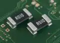


Thick film chip resistors are the default general‑purpose resistor technology in modern electronics, offering low cost, wide value range, and robust SMT assembly performance.
Key Takeaways
- Thick film chip resistors serve as the default general-purpose resistor technology in modern electronics due to their low cost and robust performance.
- They have a wide resistance range (1 Ω to 100 MΩ) but exhibit higher noise and drift compared to thin film.
- The construction involves a fired paste on a ceramic substrate and includes processes like screen printing and laser trimming.
- Thick film networks are advantageous for applications requiring multiple resistors, offering better ratio matching and simplified logistics.
- For general designs, choose thick film, upgrading to thin film only for specific accuracy or noise requirements.
This guide translates core technology and comparison content into practical design rules for selecting and using thick film chip resistors and networks.
Thick Film Resistors as the Workhorse Technology
Thick film (metal glaze) resistors use a fired paste of noble‑metal oxides and glass on a ceramic substrate, forming a few‑ to tens‑of‑micrometres thick resistive layer. This granular conduction network supports very high sheet resistance (up to about 1 MΩ/□), enabling high resistance values in compact chip sizes.
Key characteristics for “workhorse” use:
- Very wide resistance range (typically 1 Ω to 100 MΩ for chip styles).
- Standard tolerances of 1–5%, TCR from about ±50 to ±200 ppm/°C (up to ±300 ppm/°C on inexpensive series).
- Inherently good moisture robustness due to glassy, sintered film directly bonded to alumina.
- Higher noise, non‑linearity, and drift than thin film, but adequate for most industrial, consumer, and automotive designs.
Use thick film as your default in cost‑sensitive, medium‑precision, and high‑volume applications unless specific limits (noise, linearity, stability, or HF behaviour) force a thin‑film or foil alternative.
Thick Film Chip Resistor Construction and Process
A standard thick film chip resistor consists of:
- 96% alumina substrate.
- Screen‑printed inner terminations.
- Screen‑printed resistive paste (RuO₂ or similar) fired to form the thick film.
- Laser‑trimmed resistor geometry.
- Passivation (glass/epoxy) over the element.
- Nickel barrier and matte tin outer terminations.
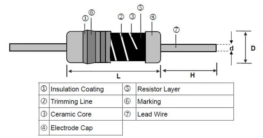
Process Outline
- Screen print inner conductors, dry, and fire.
- Screen print resistive element in defined pattern, dry, then fire at high temperature so the glass frit sinters and bonds to the substrate.
- Measure and laser‑trim each part up in resistance from a slightly low pre‑trim value; trimming lengthens the current path.
- Screen print and cure passivation layer; mark larger case sizes.
- Apply Ni barrier via sputtering and plate 100% matte Sn for soldering.
Laser trimming of thick film creates local microcracks around the cut due to poor thermal conductivity of the glassy film, which contributes to higher noise, worse TCR, and higher drift compared with thin film.
SMD Chip Resistor Types
SMD resistor technology has diversified far beyond basic thick‑film chips, and choosing the right type is often more critical than simply picking an exact resistance value. The overview below summarizes the most common categories and their typical use cases.
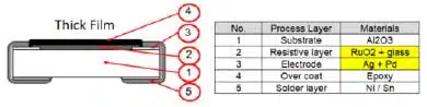
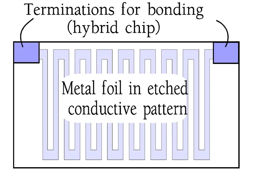
The predominant part of all chips are manufactured with thick film, but thin film chips are becoming more and more common. Also metal foil exists as SMD. The construction is like the one in Figure 5. Certain types have an organic protection in one or two layers on top of the glass passivation.
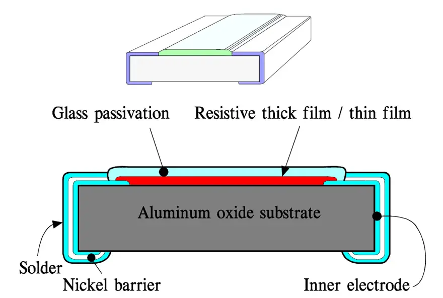
The substrates are screen printed either with a metal powder paste that is fired to a metal glaze / thick film. Or metal foils are glued on a substrate or metal films are vaporized or ion implanted on it.
The thick film is laser trimmed to the right resistance value by cutting a track in the long side of the film. Recent manufacturing improvements however begin making this laser trimming unnecessary. This approach without any trimming tracks will increase the pulse load capability by 2 to 3 times. The other films are designed to an inductance-reducing serpentine pattern according to Figure 4. and 5.
The metal foil pattern is etched chemically or patterned by means of an ion beam. The thin metal films are applied through a mask to the desired shape.
Package Sizes, Power Ratings and Derating
Chip size, substrate material, and terminations define the power rating and voltage capability of thick film resistors. Standard ratings assume a defined maximum hot‑spot temperature (often 125–155 °C) and free‑air mounting on FR‑4.
Typical Chip Sizes and Nominal Power Ratings (Example)
| Chip size | Nominal power at 70 °C | Typical Umax (DC) | Notes |
|---|---|---|---|
| 0201 | 0.05 W | 25–50 V | Very small, assembly‑critical. |
| 0402 | 0.063–0.1 W | 50–75 V | High‑density logic, RF. |
| 0603 | 0.1–0.25 W | 50–100 V | General purpose. |
| 0805 | 0.125–0.25 W | 100–150 V | Workhorse size. |
| 1206 | 0.25–0.5 W | 150–200 V | Higher voltage/power. |
| 1210+ | 0.5–1 W+ | Up to 200 V+ | Power or surge series. |
(Use actual values from chosen manufacturer datasheets; numbers above are typical design‑guide figures rather than specifications.)
Power derating
- Power rating is specified at a reference ambient (often 70 °C) and linearly derated to zero at the maximum specified ambient (for example 155 °C).
- High‑power and AlN‑substrate thick film series can support significantly higher surface load W/mm² and power ratings; always follow the vendor’s derating curves.
- Nomographic load charts (as shown for generic film resistors) relate power, ambient temperature, hot‑spot temperature, operating time, and expected resistance drift; conservative derating (for example to 40–60% of nominal power) is necessary for high stability or high‑reliability designs.
Thick Film Networks and Arrays
Thick film technology naturally lends itself to resistor networks and arrays because multiple resistive elements can be screen‑printed on a single substrate before singulation or encapsulation.
Typical network types:
- Isolated arrays (same or different values, separate resistors).
- Bussed (one common node, individual taps).
- Ladder / R‑2R digital‑to‑analog structures.
- Custom networks integrated with other thick‑film components (for example jumpers, fuses, terminations).
Advantages:
- Better ratio matching than discrete components, because elements share substrate, firing, and environment.
- Reduced PCB area and placement cost.
- Simplified BOM and logistics.
Use thick film networks for pull‑up/pull‑down arrays, address/data bus terminations, voltage dividers, and moderately accurate analog functions where absolute tolerance demands are moderate but ratio matching is important.
Typical Electrical Parameters and Tolerances
Thick film parameters are determined by paste formulation, film thickness, geometry, and trimming strategy.
Typical Parameter Ranges (Chip Series)
| Parameter | Typical thick film range | Notes |
|---|---|---|
| Resistance range | 1 Ω – 100 MΩ | Higher values possible in HV series. |
| Tolerance | ±1%, ±2%, ±5% | ±0.5% and tighter exist on premium lines. |
| TCR | ±50 to ±200 ppm/°C | Up to ±300 ppm/°C on low‑cost, ±25 ppm/°C available with caution. |
| Max operating temperature | 125–155 °C | Check series‑specific limits. |
| Max working voltage (chips) | 50–200 V | Depends on size and resistance. |
Design rules:
- Avoid designing right at the series maximum resistance and maximum voltage; allow margin for future sourcing and stability.
- For ±25 ppm/°C options, check long‑term drift data; these can drift outside the nominal TCR window under harsh conditions.
- For very low values (<10 Ω), ensure you are using a dedicated low‑ohmic thick‑film or metal‑element shunt series; standard thick film parts at very low values may have poor TCR and high current noise.
Noise, Voltage Coefficient and Stability Limits
Noise and non‑linearity
Conduction in thick film is via inter‑granular contact networks, which introduces excess 1/f noise and non‑linearity.
- Current noise is significantly higher than in thin film for the same resistance value, particularly for high‑value parts.
- Third‑harmonic distortion is much worse: typical non‑linearity is >50 dB for thick film versus >110 dB for thin film.
- Laser trimming damage (microcracks) further increases noise and drift near trimmed regions.
Avoid thick film in low‑noise amplifiers, precision ADC/DAC front ends, or audio paths; thin film or foil is preferred there.
Voltage coefficient of resistance (VCR)
- Thick film exhibits a stronger voltage coefficient than thin film, meaning resistance changes with applied voltage (field strength).
- At high voltage or where linearity matters (precision dividers, measurement chains), quantify VCR and its effect on gain error.
Stability limits
Long‑term stability of thick film is limited by:
- Granular conduction structure and microcracks.
- Diffusion and structural relaxation under high temperature.
- Moisture and ionic contamination at interfaces.
Typical long‑term drift for 1% thick film parts at rated conditions is several tenths of a percent over thousands of hours, worse than thin film by roughly an order of magnitude for the same operating stress. For high‑reliability or metrology designs, derate voltage and power aggressively and consider thin film or foil.
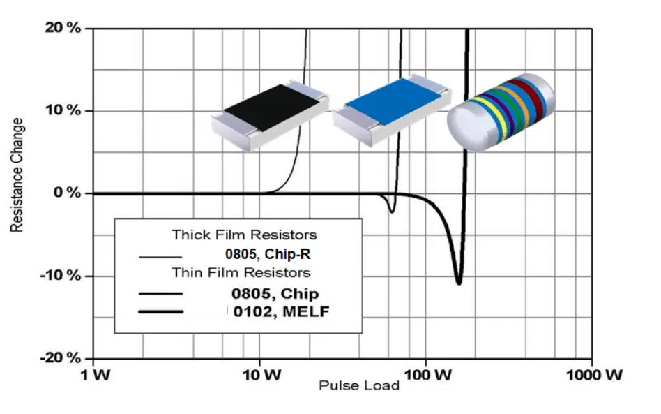
Pulse Load and Surge Capability of Thick Film Resistors
Pulse behaviour is a key differentiator between resistor technologies.
- Thick film is generally superior to thin film for very short pulses (≤100 µs) in terms of energy handling per area.
- Thin film, thanks to better heat conduction in the metallic layer, can outperform thick film for longer pulses where thermal diffusion into the substrate dominates.
- MELF geometries provide the best pulse capability due to longer current path and larger effective surface area compared with equivalent chip sizes.
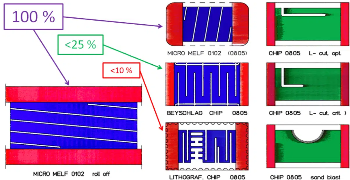
MELF capacitors that are also available in (micro)-chip case sizes have its advantage with possible path around the whole chip that makes it more efficient compare to Thick/Thin film SMDs. See the current path example on 0805 chip equivalent in Figure 6. below and pulse load capability comparison in Figure 7.:
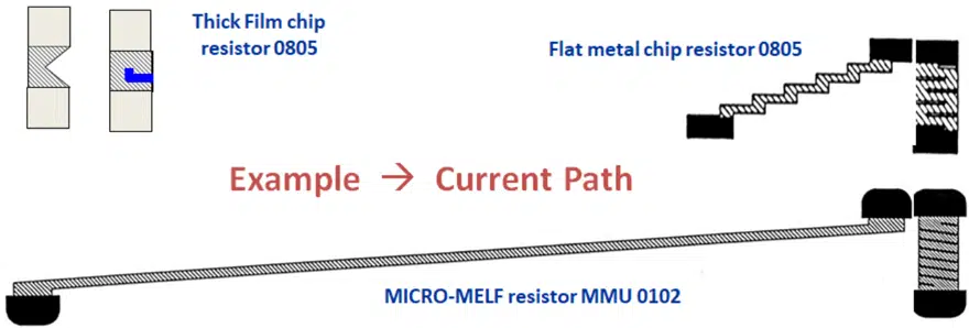
The differences in effective current length path are also reflected in the possible surface loads [W/mm2]. See the Figure 8. below.
Figures comparing thick film, thin film, and MELF 0805‑equivalent parts show:
- Longer current path and higher allowable surface load for MELF versus chip shapes.
- Higher allowable relative surface load W/mm² for thick film versus thin film at very short pulse durations.
Design guidelines:
- Always use manufacturer’s pulse‑load curves; pulses up to many times rated power are acceptable if the duration and repetition rate keep average power within limits and the instantaneous energy below the specified curve.
- For surge or inrush protection, choose dedicated “surge” or “pulse‑proof” thick film series with reinforced film and terminations.
- Keep pulse energy local to un‑trimmed regions whenever possible (for example avoid heavy surge across heavily trimmed high‑value parts).
Failure Modes and Reliability Considerations
Common failure and degradation mechanisms for thick film chip resistors include:
- Open circuits due to cracked terminations, solder joint failure, or severe overload burning off the film.
- Resistance increase from microcrack growth, film damage under pulse load, or high‑temperature operation.
- Resistance decrease from contamination or conductive paths across the surface in high humidity or dirty environments (less common due to good moisture robustness of the glassy film).
- Parametric shifts from long‑term diffusion and stress relaxation, aggravated by high temperature, high voltage, and high humidity.
Reliability design rules:
- Derate power (for example run at 30–60% of rated power for long‑life applications).
- Derate voltage, especially for high‑value parts; observe creepage and clearance on the PCB.
- Avoid operating near maximum temperature rating; consider 125 °C hot spot as a practical upper limit for long‑life designs, even if 155 °C is allowed.
- For safety‑critical circuits where open‑circuit failure must be avoided, consider series/parallel combinations or alternative technologies (for example homogeneous carbon composition, or redundant networks), depending on standards.
PCB Layout Guidelines for Chip Resistors
PCB layout strongly influences thermal behaviour, solder‑joint reliability, and parasitic effects.
Key guidelines:
- Land patterns: follow the resistor manufacturer’s recommended pad dimensions and solder mask openings; excessive pad size increases solder volume and risk of tombstoning.
- Thermal balance: ensure symmetrical copper areas on both terminals to avoid skewed wetting forces and tombstoning, especially on small sizes (0201–0603).
- Current handling: for high current, widen traces to reduce I²R loss and ensure the copper width matches the resistor’s current capability (for low‑value shunts, refer to dedicated shunt guidelines).
- High voltage: increase creepage distance between pads and to adjacent conductors; avoid solder mask slivers that can trap contamination.
- Thermal coupling: avoid placing sensitive thick film resistors directly adjacent to hot components; keep sufficient spacing or provide thermal relief to minimise temperature gradients.
- Mechanical stress: do not place resistors across PCB slots, panel v‑grooves, or board edges; these areas see higher bending stress and can crack chips.
For wave soldering of larger chip sizes, use pad geometries and solder volume that minimise tombstoning; reflow is preferred for small case sizes.
High‑Voltage and High‑Frequency Design Aspects
High‑voltage aspects
Thick film is frequently used in high‑ohmic and high‑voltage resistors due to the possibility of very high sheet resistance and good environmental robustness.
Design points:
- Observe both maximum working voltage and overload voltage from datasheets; do not exceed either limit.
- For very high voltage dividers, use larger chip sizes, series chains of resistors, or dedicated HV thick‑film parts with extended creepage and optimised geometry.
- Consider voltage coefficient and its effect on accuracy in high‑voltage measurement dividers.
- Control surface contamination and humidity with conformal coating or proper creepage distances; even glassy thick film can be compromised by surface leakage across the PCB.
High‑frequency aspects
Spiralling and geometry introduce parasitics similarly to other film resistors:
- Small‑value chips (<100 Ω) tend to be inductive.
- Mid‑range values (about 100–470 Ω) are approximately resistive.
- Higher values become increasingly capacitive.
Additional HF considerations:
- MOSFET gate resistors and RF bias networks often use thick film chips successfully if parasitic inductance and capacitance are tolerable.
- For very high‑frequency or very low‑distortion RF applications, thin film or special RF resistor series may be required.
- MELF parts can offer improved HF performance due to more favourable current paths and reduced inductance.
Typical Applications for Thick Film Resistors
Representative use‑cases where thick film is usually preferred:
- General‑purpose pull‑ups/pull‑downs and bias networks in digital and mixed‑signal designs.
- Load, sense (moderate accuracy) and damping resistors in power supplies and converters.
- Input and feedback resistors where 1–2% tolerance and modest drift are acceptable.
- LED current limiting in consumer and industrial equipment.
- Automotive ECUs where cost, temperature range, and moisture robustness matter more than metrology‑grade stability, often in qualified AEC‑Q200 thick film series.
- Resistor arrays for bus terminators, series damping, and general I/O conditioning.
Avoid thick film for:
- Precision instrumentation amplifiers, gain‑setting networks for 16‑bit+ converters, or precision reference dividers.
- Lowest‑noise audio paths and low‑level sensor front ends.
- Circuits demanding ppm‑class long‑term stability or ultra‑low TCR over wide temperature spans.
When to Prefer Thick Film over Thin Film
The table below summarises key selection criteria.
Thick Film vs Thin Film Selection Matrix
| Design aspect | Prefer thick film when… | Prefer thin film when… |
|---|---|---|
| Cost | BOM cost is strongly constrained. | Budget allows premium per resistor. |
| Tolerance | ±1–5% is sufficient. | You need ±0.1–0.5% or better. |
| TCR | ±50–200 ppm/°C is acceptable. | You target ±5–25 ppm/°C over wide range. |
| Long‑term stability | Drift of several 0.1% is acceptable. | You need tightly controlled long‑term drift. |
| Noise / linearity | Circuit is not noise‑critical and tolerates distortion. | Low noise and high linearity are critical (ADC/DAC, audio). |
| Moisture environment | High humidity or condensation likely. | Controlled environment or special moisture‑robust thin film is used. |
| Pulse load (short) | Very short surge pulses dominate (≤100 µs). | Longer pulses or repetitive high energy pulses. |
| HF behaviour | Moderate HF, non‑critical parasitics. | High‑frequency precision or RF gain/attentuation. |
Rule‑of‑thumb: start with thick film for general designs, then upgrade specific positions to thin film or foil only where measurement data or requirements justify it.
Links to Thin Film and Selection/Benchmark Guides
For complementary design information and technology comparison, link from this thick film design guide to:
- Thin Film and Metal Film Resistors Thin / metal film resistor technology overview and construction details
- Resistor, What is it ? – The basic resistor technology introduction
- Resistor Types and Construction Fundamentals – Thin vs thick film resistor comparison charts for TCR, tolerance, stability, noise, non‑linearity, and pulse capability, including the domain diagram of film thickness versus square resistance.
These cross‑links help readers quickly navigate from this thick film‑focused document to precision thin‑film design topics and broader resistor selection methodologies.
Conclusion
Thick film resistors represent the most cost-effective and versatile resistor technology for general-purpose electronic design. Their wide resistance range (1 Ω to 100 MΩ), excellent moisture robustness, and superior pulse capability make them the default choice for the vast majority of applications in consumer, industrial, and automotive electronics.
While thick film technology has inherent limitations in noise performance, long-term stability, and voltage coefficient compared to thin film, these characteristics are more than adequate for most circuit requirements. The key to successful design is understanding when thick film’s workhorse attributes are sufficient and when specific circuit demands—ultra-low noise, tight tolerance matching, or metrology-grade stability—justify the premium cost of thin film alternatives.
By following the design rules and selection criteria outlined in this guide, engineers can confidently specify thick film chip resistors for their projects, optimizing cost and performance while maintaining reliability across the full range of operating conditions. Start with thick film as your default, then upgrade specific positions only where measurement data or requirements clearly justify it.
FAQ: Thick Film Resistors
Thick film resistors use a fired paste of noble-metal oxides (typically RuO₂) and glass on a ceramic substrate, forming a resistive layer several to tens of micrometers thick. This granular conduction network creates a robust, cost-effective resistor with a wide resistance range (1 Ω to 100 MΩ) suitable for general-purpose electronics.
Use thick film resistors when:
BOM cost is strongly constrained
Tolerances of ±1-5% are sufficient
TCR of ±50-200 ppm/°C is acceptable
Circuits are not noise-critical
High humidity or moisture environments are expected
Very short surge pulses (≤100 µs) need to be handled
Power ratings depend on chip size:
0201: 0.05 W
0402: 0.063-0.1 W
0603: 0.1-0.25 W
0805: 0.125-0.25 W (workhorse size)
1206: 0.25-0.5 W
1210+: 0.5-1 W+
Ratings are specified at reference ambient (often 70°C) and must be derated linearly to zero at maximum temperature (typically 155°C).
Thick film resistors have higher noise, worse non-linearity (>50 dB vs >110 dB for thin film), higher voltage coefficient, and greater long-term drift compared to thin film. They are not suitable for precision instrumentation, low-noise audio paths, or circuits requiring ppm-class stability.
MELF (Metal Electrode Leadless Face) resistors have cylindrical geometry with longer current paths around the entire component, providing superior pulse load capability and higher allowable surface load (W/mm²) compared to rectangular chip resistors. MELF designs offer better performance for surge protection and high-energy pulse applications.
Start with thick film as your default for general designs due to lower cost and robust performance. Upgrade to thin film only for specific positions requiring ultra-low noise (ADC/DAC front ends, audio paths), tight tolerance (±0.1-0.5%), ultra-low TCR (±5-25 ppm/°C), or metrology-grade long-term stability.
Thick film networks are multiple resistive elements screen-printed on a single substrate, available as isolated arrays, bussed configurations, or R-2R ladder structures. Use them for pull-up/pull-down arrays, bus terminations, and voltage dividers where ratio matching is more important than absolute tolerance, offering reduced PCB area and simplified logistics.
How to Select and Specify Thick Film Chip Resistors
- Step 1: Determine Your Resistance Range and Tolerance Requirements
Start by defining your target resistance value (1 Ω to 100 MΩ) and acceptable tolerance. Standard thick film offers ±1%, ±2%, or ±5% tolerance. If you need ±0.1-0.5% or tighter, consider thin film instead.
- Step 2: Calculate Power Dissipation and Select Package Size
Calculate I²R power dissipation in your circuit. Select a chip size that keeps you at 40-60% of nominal power rating for high-reliability designs. Remember: 0603 and 0805 are general-purpose workhorse sizes; 1206+ for higher power applications.
- Step 3: Verify Temperature Coefficient of Resistance (TCR) Requirements
Check if ±50 to ±200 ppm/°C TCR is acceptable for your application temperature range. If you need ±5-25 ppm/°C over wide temperature spans, thick film is insufficient—upgrade to thin film.
- Step 4: Evaluate Voltage Rating and High-Voltage Considerations
Confirm that the chip size and resistance value support your maximum working voltage (typically 50-200 V for standard chips). For high-voltage dividers, use larger sizes, series chains, or dedicated HV thick film parts with extended creepage.
- Step 5: Check Noise and Linearity Requirements
Assess whether your circuit is noise-sensitive. Avoid thick film in low-noise amplifiers, precision ADC/DAC front ends, or audio paths where excess 1/f noise and >50 dB non-linearity are problematic. For these applications, specify thin film or foil resistors.
- Step 6: Review Pulse Load and Surge Capability
If your application involves surge protection or inrush current, consult manufacturer pulse-load curves. Thick film excels at very short pulses (≤100 µs). For dedicated surge applications, choose “surge-proof” or “pulse-proof” series with reinforced construction.
- Step 7: Consider Environmental and Long-Term Stability Requirements
Evaluate operating environment: thick film offers excellent moisture robustness due to glassy sintered film. However, expect several tenths of a percent drift over thousands of hours at rated conditions. For metrology-grade stability, derate aggressively or switch to thin film.
- Step 8: Optimize PCB Layout for Thermal and Mechanical Performance
Follow manufacturer land patterns for pad dimensions. Ensure symmetrical copper areas on both terminals to prevent tombstoning. For high-power applications, widen traces to reduce I²R loss. Maintain adequate creepage for high-voltage designs and avoid placing resistors across PCB slots or panel edges.
- Step 9: Apply Derating for High-Reliability Designs
Conservative derating is essential: operate at 30-60% of rated power, stay below 125°C hot-spot temperature, and allow voltage margin. Check vendor derating curves and follow nomographic load charts for your specific operating conditions.
- Step 10: Source from Qualified Manufacturers and Verify Specifications
Select resistors from manufacturers offering AEC-Q200 qualification for automotive applications or appropriate quality standards for your industry. Always verify actual datasheet values rather than using typical design-guide figures.