


This article based on Würth Elektronik webinar presentation discusses in-depth optimizing RF signal integrity for coaxial connectors and coaxial-to-PCB interconnect.
This Würth Elektronik Webinar presentation and the article provides a comprehensive technical analysis of coaxial-to-planar transitions, connector mechanics, and regulatory compliance.
Key Takeaways:
- Critical inch from coax to PCB defines RF performance: The transition from a coaxial connector to the PCB over just a few millimeters is the dominant source of impedance discontinuity and RF signal degradation in high‑frequency designs.
- Accurate impedance modeling prevents reflections and loss: Understanding coaxial TEM propagation, the correct 60/138 impedance formulas, dielectric effects, VSWR and return loss is essential to minimize reflections, standing waves and wasted transmitter power.
- Connector geometry and mechanics strongly influence signal integrity: SMA architecture, contact captivation, plating choices and the use of round posts versus flat tabs directly affect impedance continuity, skin‑effect losses, passive intermodulation and achievable VSWR.
- CPWG, via fences and careful pad design improve matching: Using coplanar waveguide with ground, dense via fences, tapered traces, solder mask keep‑out and optimized pad geometry allows engineers to closely emulate the coaxial field distribution on the PCB.
- Defected ground structures and solder control tune real‑world impedance: Removing ground under pads with DGS and managing solder volume compensates parasitic capacitance so that the assembled connector‑to‑PCB interface approaches a 50 Ω match.
- Miniature RF connectors require strict handling: Ultra‑miniature UMRF/U.FL style connectors offer compact 50 Ω interconnects up to about 6 GHz but are limited in mating cycles and demand tool‑assisted, vertical insertion and removal.
- PFAS and PTFE regulations impact connector materials: Upcoming PFAS restrictions increase compliance and reporting demands for PTFE‑based RF connectors and may drive alternative dielectrics or exemptions for critical electronic infrastructure.
- Assembly quality is as important as the RF design: Stencil aperture control, segmented solder pads, solder‑mask clearances and correct SMA torque are mandatory to translate a simulated 50 Ω design into repeatable hardware performance.
Introduction
The transmission of high-frequency signals represents one of the most sophisticated challenges in modern electronics engineering. As the global demand for bandwidth accelerates—driven by the proliferation of 5G networks, the Internet of Things (IoT), and high-speed data protocols—the margin for error in Radio Frequency (RF) design has effectively vanished. Central to this challenge is the physical interface where the signal transitions from a coaxial cable to a Printed Circuit Board (PCB). This transition point, often spanning mere millimeters, acts as a critical gateway that determines the efficiency, integrity, and reliability of the entire RF chain. It is here, in the “critical inch,” that the theoretical elegance of Maxwell’s equations meets the harsh realities of manufacturing tolerances, material science, and mechanical constraints.
This article provides an examination of the coaxial-to-PCB interconnect. We move beyond simple datasheet specifications to explore the underlying electromagnetic physics that govern impedance matching, signal reflection, and loss mechanisms. We analyze the mechanical evolution of the SMA connector, contrasting traditional designs with modern, optimized geometries like the Flat Tab, and delve into the miniature world of UMRF interconnects. Furthermore, we investigate advanced PCB layout techniques, including Defected Ground Structures (DGS) and tapered transmission lines, providing a roadmap for achieving superior Voltage Standing Wave Ratio (VSWR) performance.
This article also addresses the looming regulatory transformation reshaping the materials landscape. With the impending restrictions on Per- and Polyfluoroalkyl Substances (PFAS), specifically Polytetrafluoroethylene (PTFE)—the ubiquitous dielectric of the RF world—engineers must now navigate a complex compliance environment. We provide a detailed analysis of the 2025 regulatory horizon, offering strategic insights for supply chain resilience. This document serves as a definitive resource for RF architects, compliance officers, and layout engineers dedicated to mastering the art of high-frequency signal transport.
Chapter 1: The Physics of Coaxial Transmission and Impedance
The Electromagnetic Foundation
To optimize the transition from a cable to a circuit board, one must first understand the fundamental physics of the coaxial line itself. The coaxial cable is a transmission line consisting of two concentric conductors separated by a dielectric insulator. This geometry supports a Transverse Electromagnetic (TEM) mode of propagation, where both the electric and magnetic fields are perpendicular to the direction of wave travel. The efficiency of this structure was first mathematically described by Oliver Heaviside in his 1880 British patent, where he demonstrated how the coaxial configuration could eliminate signal interference and crosstalk, a principle that remains the bedrock of RF engineering today.1
The defining characteristic of any transmission line is its characteristic impedance Z0, a parameter that represents the ratio of voltage to current for a wave traveling in a single direction. In a lossless line, this impedance is purely resistive, but strictly dependent on the physical dimensions of the conductors and the dielectric properties of the insulation. The impedance determines how energy flows through the system; any deviation from the system’s characteristic impedance typically 50Ω or 75Ω results in energy reflection, manifesting as signal loss and potential damage to sensitive source components.
Deriving the Impedance Formula: The “138” vs. “60” Constant
A source of frequent confusion in RF engineering resources is the variation in the constants used to calculate coaxial impedance. Engineers often encounter formulas using either “138” or “60” as the scalar multiplier. Understanding the derivation of these constants is essential for precise modeling, particularly when designing custom PCB transitions or interpreting legacy data.
The fundamental formula for the characteristic impedance Z0 of a coaxial cable is derived from the capacitance C and inductance L per unit length:
For a coaxial geometry with an inner conductor diameter d and an outer shield inner diameter D, filled with a dielectric of relative permittivity εr, the inductance and capacitance are given by:
Substituting these into the impedance equation, and assuming a non-magnetic dielectric µr, the equation simplifies to its natural logarithm form:
The term represents the impedance of free space, which is approximately 376.7 Ω . Dividing this by yields approximately 59.95, which is rounded to 60. Thus, the scientifically rigorous formula using the natural logarithm ln is:
However, historically, engineering calculations were performed using base-10 logarithms log10 for ease of manual computation. The conversion factor between the natural logarithm and the base-10 logarithm is approximately 2.3026. . When we multiply the constant 60 by 2.3026, we arrive at approximately 138.15.
This leads to the common “engineering” version of the formula found in many datasheets and older textbooks:
Insight: While both formulas yield the same result, the choice of formula implies the logarithmic base. Using the constant 138 with a natural logarithm, or 60 with a base-10 logarithm, will result in catastrophic calculation errors (an impedance error factor of roughly 2.3x). For modern computational modeling and simulation, the natural logarithm form (using 60) is preferred as it aligns directly with Maxwell’s equations.
Dielectric Constants and Phase Velocity
The presence of the dielectric material εr fundamentally alters the speed at which signals propagate through the cable. This velocity of propagation Vp is inversely proportional to the square root of the dielectric constant:
Where c is the speed of light in a vacuum ().
For solid PTFE (Teflon), the standard dielectric for SMA connectors, εr is approximately 2.1. This results in a propagation velocity of roughly 69% of the speed of light. This reduction in speed, and the corresponding reduction in wavelength inside the component, is critical for layout design. A PCB trace length that appears electrically short in air may be electrically long (and thus resonant) when the fields are traveling through the dielectric of a connector or the FR4 substrate of a board.
Designers must also consider the cutoff frequency. A coaxial cable supports TEM mode propagation only up to a frequency where the wavelength becomes comparable to the transverse dimensions of the cable. Above this cutoff frequency, higher-order waveguide modes can propagate, causing unpredictable impedance and signal distortion. The cutoff frequency is inversely proportional to the diameter of the outer conductor. This physics drives the connector industry’s evolution: as frequencies rise, connectors must shrink. This is why 2.92mm connectors work to 40 GHz, while standard SMAs are typically limited to 18 GHz.
Chapter 2: Signal Integrity Metrics: The Language of Loss
Understanding Reflections and Discontinuity
When a high-frequency signal encounters a change in impedance—such as the transition from a connector pin to a PCB trace—a portion of the energy is reflected back toward the source. This phenomenon is analogous to light hitting a window; some passes through (transmission), and some bounces back (reflection). In RF systems, these reflections form standing waves, where forward and reverse waves interfere constructively and destructively.
The magnitude of this reflection is quantified by the Reflection Coefficient , which is determined by the impedance mismatch:
Where ZL is the load impedance (the PCB interface) and Z0 is the characteristic impedance of the system 50Ω.
Voltage Standing Wave Ratio (VSWR)
The Voltage Standing Wave Ratio (VSWR) is the traditional metric for quantifying mismatch. It measures the ratio of the maximum voltage to the minimum voltage along the transmission line. A VSWR of 1:1 implies a perfect match (no reflection), while a VSWR of ∞ implies total reflection (open or short circuit).
Würth Elektronik’s technical literature categorizes VSWR values into performance tiers for Coaxial Systems:
- 1.0 (Very well matched): Theoretical perfection.
- 1.1 – 1.2 (Well matched): High-performance laboratory and aerospace grade.
- 1.2 – 1.3 (Matched): Standard target for good commercial RF design.
- 1.5 (Poorly matched): Acceptable for some low-cost consumer applications but incurs noticeable loss.
- > 2.0 (Not matched): Indicates a failure in design, leading to significant power loss and potential transmitter instability.
Return Loss (RL): The Decibel Perspective
While VSWR is useful for visualizing standing waves, Return Loss (RL) is often preferred for link budget calculations as it expresses the reflected power in decibels (dB).
The relationship between VSWR and Return Loss is non-linear. As the table below demonstrates, improving VSWR from 1.3 to 1.2 yields a greater gain in signal purity than improving from 1.5 to 1.4.
Table 1: Comprehensive VSWR to Return Loss Conversion
| VSWR (:1) | Return Loss (dB) | Reflection Coefficient (Γ) | Reflected Power (%) | Signal Integrity Context |
| 1.00 | ∞ | 0.000 | 0.00% | Ideal / Theoretical Limit |
| 1.01 | 46.1 dB | 0.005 | 0.00% | Metrology Grade Calibration Standards |
| 1.05 | 32.3 dB | 0.024 | 0.06% | High-Precision Instrumentation |
| 1.10 | 26.4 dB | 0.048 | 0.23% | High-End Aerospace/Defense |
| 1.15 | 23.1 dB | 0.070 | 0.49% | Excellent Commercial Performance |
| 1.20 | 20.8 dB | 0.091 | 0.83% | Target for Quality PCB Transitions |
| 1.25 | 19.1 dB | 0.111 | 1.23% | Good Acceptable Limit |
| 1.30 | 17.7 dB | 13.0% | 1.70% | Acceptable for Standard Wi-Fi/Consumer |
| 1.40 | 15.6 dB | 0.167 | 2.78% | Marginal Performance |
| 1.50 | 14.0 dB | 0.200 | 4.00% | Poor – Significant Signal Degradation |
| 1.70 | 11.7 dB | 0.259 | 6.72% | Very Poor |
| 2.00 | 9.5 dB | 0.333 | 11.11% | System Failure / Mismatch |
| 3.00 | 6.0 dB | 0.500 | 25.00% | 25% Power Lost to Reflection |
Insight: A Return Loss of 20 dB (VSWR ~1.22) is widely regarded as the “gold standard” for PCB-to-connector transitions. Achieving this requires precise matching. If a connector has a Return Loss of 10 dB (VSWR ~1.9), 10% of the power is reflected. In a high-power transmitter (e.g., 100 Watts), this means 10 Watts is bouncing back into the amplifier, potentially causing overheating or catastrophic failure.
Chapter 3: Connector Anatomy and Mechanics
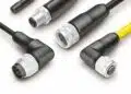
The SMA Connector Architecture
The Sub-Miniature Version A (SMA) connector is the ubiquitous workhorse of the RF industry. Developed in the 1960s, it utilizes a threaded coupling mechanism (1/4-36 UNS) to provide mechanical stability and excellent electrical performance up to 18 GHz, with precision variants extending to 26.5 GHz.
The connector comprises three primary elements:
- The Body: Acts as the outer conductor and ground reference. It is typically machined from brass or stainless steel.
- The Center Contact: The active signal carrier, usually made of Beryllium Copper (BeCu) or brass, plated with gold.
- The Insulator: A dielectric spacer, almost exclusively PTFE, which maintains the concentricity of the center contact relative to the body.
Captivation Mechanisms
A critical but often overlooked aspect of connector design is captivation. This refers to the mechanical features that prevent the center contact and insulator from moving axially or rotationally within the body. Movement can occur due to thermal cycling (expansion/contraction) or mechanical mating forces. If the center pin shifts, the impedance profile changes, and the connection to the PCB can be severed.
There are several captivation technologies such as:
- Barb: A barb on the center contact digs into the soft PTFE dielectric. Simple but can degrade the dielectric.
- Epoxy: Using adhesive to bond the components. Effective but limits temperature range.
- Knurls: Straight or crossed knurls on the contact create friction against the dielectric.
- Mechanical Shoulders: A widening of the contact that sits against a step in the insulator. This is the most robust method for high-performance connectors.
Pin Geometry: Round Post vs. Flat Tab
The interface where the connector meets the PCB is the primary source of impedance discontinuity. Manufacturers like Würth Elektronik offer two distinct center contact “back shapes” for End Launch and Edge Mount connectors: the Round Post and the Flat Tab. The choice between these significantly impacts PCB layout requirements.
1. Round Post (Blunt Post)
- Description: The center pin extends as a solid cylinder.
- Mechanical Advantage: The round profile is structurally robust and resistant to bending during assembly or handling. It provides a large surface area for the solder fillet.
- Electrical Disadvantage: The geometric mismatch is severe. A typical round post might have a diameter of 1.27mm. On a standard 1.6mm FR4 PCB, a 50Ω microstrip trace might be only 0.3mm wide. Connecting a 1.27mm pin to a 0.3mm trace creates a massive capacitive step.
- Implication: To use a Round Post effectively, the PCB layout requires aggressive compensation (tapering or DGS) to neutralize the excess capacitance.
2. Flat Tab
- Description: The center contact is flattened into a rectangular tab.
- Electrical Advantage: The flat geometry mimics the planar nature of the PCB trace. The tab width is often designed to be closer to the width of a standard 50Ω line on typical substrates. This minimizes the “step” in geometry, reducing parasitic capacitance and preserving impedance continuity.
- Performance: Flat Tab connectors generally yield superior Return Loss performance at frequencies above 5 GHz, requiring less aggressive layout compensation than their round counterparts. They are the preferred choice for high-frequency data transmission.
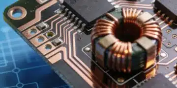
Plating and the Skin Effect
At microwave frequencies, current does not flow through the entire cross-section of the conductor. Instead, it is confined to a thin layer on the surface, a phenomenon known as the Skin Effect.
- Skin Depth δ : The depth at which the current density falls to (about 37%) of its surface value. At 1 GHz, the skin depth in copper is approximately 2.1 micrometers. At 10 GHz, it shrinks to 0.66 micrometers.
Because current flows only in this microscopic skin, the plating material of the connector becomes the primary conductor.
- Gold: The standard for center contacts. It has excellent conductivity and, crucially, does not oxidize.
- Nickel: Often used as an underplate or on the outer body. However, nickel is ferromagnetic . This increases the skin effect resistance and can generate Passive Intermodulation (PIM) distortion.
- Optimization: For high-precision or high-power applications, “non-magnetic” connectors are specified. These use white bronze or silver plating, or apply gold directly over copper, eliminating the nickel layer to prevent magnetic losses.
Chapter 4: PCB Transmission Line Architectures
To successfully integrate a coaxial connector, the PCB must provide a transmission line structure that matches the electromagnetic mode of the coax as closely as possible.
Microstrip Line (MSL)
The Microstrip is the most common RF trace structure. It consists of a signal conductor on the top layer of the PCB, separated from a solid ground plane on the bottom layer by the dielectric substrate.
- Field Distribution: The electric field lines extend from the trace down to the ground plane, but a significant portion also extends up into the air. This “fringing field” means the effective dielectric constant is a mix of the substrate ).
- Drawbacks for Connectors: The ground reference is on the bottom layer. An Edge Mount connector usually has ground legs that solder to the top layer. Connecting a Microstrip requires the return current to travel through vias to reach the connector body, adding inductance.
Coplanar Waveguide with Ground (CPWG)
The Coplanar Waveguide with Ground is the superior architecture for connector interfaces. In a CPWG, ground planes are placed on the same layer as the signal trace, separated by a precise gap G, in addition to the ground plane underneath.
- Advantages for Interconnects:
- Direct Grounding: The SMA connector’s body legs solder directly to the top-layer ground planes next to the signal trace. This creates a low-inductance connection between the cable shield and the PCB ground.
- Field Confinement: The electric fields are tightly confined in the gaps between the trace and the coplanar grounds. This reduces radiation and crosstalk.
- Tunability: The characteristic impedance of a CPWG is determined by the ratio of the trace width W to the gap G. This provides an extra degree of freedom. If a connector pin requires a wide pad, the designer can maintain 50Ω by widening the gap, which is not possible with a standard Microstrip.
The Via Fence
In CPWG designs, it is critical to stitch the top ground planes to the bottom ground plane using a “Via Fence.” These vias prevent parallel plate modes from propagating between the ground layers and ensure that the top and bottom grounds remain at the same potential.
- Design Rule: The spacing (pitch) between vias should be less than (one-tenth of the wavelength at the highest operating frequency) to create an effective electromagnetic wall.
Chapter 5: The Interface Challenge (The Discontinuity)
The point where the connector pin touches the PCB pad is the single greatest source of signal degradation. This discontinuity arises from a fundamental clash of geometries and materials.
Geometric Mismatch
A 50Ω coaxial cable has a circular symmetry. A 50Ω PCB trace has a planar symmetry. Mapping one to the other involves an abrupt change in the electric field distribution.
- Capacitive Discontinuity: The soldering pad required for the connector pin is often physically larger than the transmission line width. A wider conductor over a ground plane creates a parallel plate capacitor. This “parasitic capacitance” causes the impedance to dip locally (e.g., dropping from 50Ω to 40Ω).
- Inductive Discontinuity: The pin itself, if it is long or elevated above the board (as in some through-hole designs), acts as an inductor. This causes the impedance to spike locally.
Time Domain Reflectometry (TDR) Analysis
TDR is the standard method for visualizing these discontinuities. A TDR instrument sends a fast pulse down the line and measures reflections over time (which corresponds to distance).
- The “Dip”: A capacitive discontinuity (like a large connector pad) appears as a dip in the impedance profile.
- The “Peak”: An inductive discontinuity (like a thin inductive wire or via) appears as a peak.
- Goal: The goal of optimization is to “flatten” the TDR plot, keeping the impedance line as close to 50Ω as possible throughout the transition.
Chapter 6: Optimization Strategies I: Geometric Compensation
When a standard footprint yields unsatisfactory performance (VSWR > 1.3), engineers must employ geometric compensation techniques to restore impedance matching.
Tapering (Inductive Compensation)
Tapering involves gradually changing the width of the PCB trace as it approaches the connector. This technique is essential when connecting a wide connector pin (e.g., a Round Post) to a narrow transmission line.
- The Problem: Connecting a wide, high-capacitance pin directly to a narrow line causes an abrupt impedance step.
- The Solution: The trace segment immediately adjacent to the connector pad can be made narrower than the standard 50Ω width.
- Mechanism: A narrow trace has higher inductance L and lower capacitance C. By placing a short section of high-impedance (inductive) line in series with the low-impedance (capacitive) connector pad, the two reactances can cancel each other out.
- Taper Profiles:
- Linear Taper: A straight-line transition. Simple to design but may still have discontinuities at the ends.
- Klopfenstein Taper: A curved taper that provides the optimal matching for a given length, minimizing reflection across a broad bandwidth.
- Exponential Taper: Often used to match the varying ground plane gap in CPW structures.
Trace Width Adjustment
In specific scenarios described in Würth Elektronik’s application notes, the trace width near the connector is manipulated to manage impedance.
- For Round Post: If the impedance is too low (capacitive) due to the large pin, the trace width is reduced (narrowed) at the connection point.
- For Flat Tab: If the flat pin results in lower impedance, the trace width is similarly reduced, or the gap to the coplanar ground is increased to raise the impedance.11
Chapter 7: Optimization Strategies II: Defected Ground Structures (DGS)
Defected Ground Structure (DGS) is an advanced technique that involves etching away portions of the ground plane to manipulate the transmission line’s electromagnetic properties. It is particularly effective for compensating the excess capacitance of SMA connector pads.
The Physics of DGS
The capacitance of a PCB pad is largely determined by the parallel plate formula:
Where A is the area of the pad and d is the distance to the ground plane (substrate thickness). Since the pad area A is fixed by the mechanical necessity of soldering the connector pin, the capacitance is often inherently too high for a 50Ω match.
DGS solves this by modifying the effective ground reference. By cutting a slot or “window” in the ground plane directly underneath the signal pad:
- Capacitance Reduction: The direct vertical electric field path to ground is removed. The fields must now fringe through the substrate to the edges of the ground cutout. This longer path and reduced effective area significantly lower the shunt capacitance.
- Inductance Increase: The return current flowing in the ground plane cannot cross the gap; it must divert around the cutout. This added path length increases the series inductance of the ground return.
- Impedance Elevation: Since , simultaneously increasing L and decreasing C results in a sharp increase in local impedance. This allows the designer to push the impedance of a large connector pad back up to 50Ω.
DGS Implementation & Simulation
- Shape: The cutout is typically rectangular, matching the footprint of the connector pad. More complex shapes (dumbbell, U-shape) are used for filter applications but are less common for simple impedance matching.
- Tuning: The size of the cutout is the tuning variable. A larger cutout raises the impedance more. However, making it too large can make the line highly inductive, creating a “peak” in the TDR.
- EMI Considerations: Removing the ground plane creates an aperture through which RF energy can radiate. This can cause Electromagnetic Interference (EMI) or coupling to layers below. In multi-layer boards, it is common to place a solid ground plane on a deeper layer (e.g., Layer 3) to act as a shield for the DGS on Layer 2.15
The “Tin Factor”
A critical insight from practical simulations is the impact of solder. Solder is conductive and adds volume to the joint.
- Simulation vs. Reality: A connector modeled as a dry copper contact might appear perfectly matched. However, in production, the solder fillet increases the effective surface area of the pin, adding parasitic capacitance.
- DGS Compensation: The DGS is often sized to be slightly aggressive—creating an impedance slightly above 50Ω in the dry model—so that when the capacitive solder is applied, the impedance settles exactly at 50Ω. Würth Elektronik studies confirm that the “Adjusted Shape with DGS + Tin” provides the optimal real-world match.
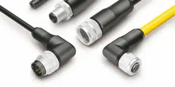
Chapter 8: Miniature Interconnects (UMRF & U.FL)
As consumer electronics shrink, the bulky SMA is often replaced by ultra-miniature connectors for internal signal routing. The U.FL standard (Hirose) and its compatible alternatives like Würth Elektronik’s UMRF (Ultra-Miniature RF) dominate this space.
Technical Specifications and Compatibility
- Impedance: 50Ω.
- Frequency Range: DC to 6 GHz. This covers all major commercial bands including Wi-Fi (2.4/5 GHz), Bluetooth, GPS, and Sub-6GHz 5G.
- Footprint: Approximately 3.0mm x 3.1mm requiring minimal board space.
- Mating Height: 2.5 mm max, making them ideal for slim devices like laptops and tablets.
- Cross-Compatibility: UMRF plugs and receptacles are fully intermateable with Hirose U.FL and I-PEX MHF1 series, simplifying supply chain management.
Assembly and Handling Limitations
Unlike the rugged SMA, UMRF connectors are delicate precision components.
- Mating Cycles: They are typically rated for only 30 mating cycles. They are designed for internal installation, not for frequent user access.
- Insertion/Extraction: Mating must be vertical. Angled insertion can crush the contact springs. Disconnection requires a specialized extraction tool (e.g., Würth Elektronik 600636001) that lifts the plug vertically. Pulling by the cable is strictly prohibited and can rip the receptacle pads off the PCB or damage the cable termination.
- Cable Diameters: Common cable options include 1.13mm, 1.32mm, and 1.37mm diameters. The choice depends on the loss budget (thicker cable = lower loss) vs. flexibility requirements.
Chapter 9: Material Science and Regulatory Compliance (PFAS)
The RF industry stands at a crossroads as global environmental regulations target “forever chemicals.” PFAS (Per- and Polyfluoroalkyl Substances) are a class of thousands of synthetic chemicals used for their resistance to heat, water, and oil. PTFE (Teflon), the primary dielectric in almost all coaxial connectors, is a fluoropolymer falling under the PFAS umbrella.
The 2025 Regulatory Horizon
Governments are moving to restrict or ban non-essential PFAS uses.
- United States (TSCA Section 8(a)(7)): The EPA has mandated reporting of PFAS usage. Manufacturers must report on PFAS manufactured or imported dating back to 2011. While the reporting deadline has seen adjustments (shifting into 2025/2026), the requirement forces deep supply chain transparency. Every connector containing PTFE must be tracked.
- Minnesota “Amara’s Law”: This state law is a bellwether for US regulation. It prohibits the sale of certain products containing intentionally added PFAS starting in 2025.
- The “Juvenile” Nuance: The law bans PFAS in “juvenile products” (for children under 12). However, it explicitly exempts children’s electronic products from this definition. This is a crucial reprieve for the electronics industry, but it signals the legislative intent to target consumer goods first.
- European Union (REACH): The European Chemicals Agency (ECHA) is evaluating a broad restriction proposal. The timeline suggests potential restrictions coming into force around 2026-2027, with debates ongoing regarding “essential use” derogations for industrial and electronic applications.
The PTFE Dilemma
Why not just replace PTFE?
- Electrical Properties: PTFE has a low dielectric constant and an extremely low loss tangent.
- Mechanical Properties: It is chemically inert and withstands high soldering temperatures.
- Impedance Dependency: The 50Ω geometry of every standard connector (SMA, BNC, N-type) is calculated based on PTFE’s εr. Switching to a material with a different dielectric constant (e.g., Nylon or LCP) would require changing the physical dimensions of the connector to maintain 50Ω. This would break backward compatibility with the billions of connectors currently in use.
- Outlook: It is highly probable that internal electronic components will receive regulatory exemptions due to the lack of viable substitutes and their critical role in communications infrastructure. However, companies must prepare for rigorous reporting requirements. The days of “ignoring” material composition are over; compliance data is now as critical as electrical data.
Chapter 10: Manufacturing and Assembly Best Practices
The best design can be ruined by poor assembly.
Solder Mask Keep-Out
Solder mask (the green coating on PCBs) is a dielectric material with a high and often uncontrolled permittivity () and high loss.
- Recommendation: Implement a strict Solder Mask Keep-Out zone over the RF trace and the gap in CPW structures. This exposes the copper (typically plated with ENIG or Immersion Silver) and ensures the fields travel through air and substrate, not the lossy mask.
Paste Stencil Design
Controlling the volume of solder is critical to controlling the “Tin Factor” capacitance.
- Aperture Reduction: For large connector pads, the stencil aperture should often be reduced (e.g., to 70-80% of the pad area) to prevent excessive solder buildup.
- Segmentation: Large pads should be segmented in the stencil (window pane effect) to prevent “scooping” and ensure an even solder height.
Connector Torque
For SMA connectors, proper mating torque is essential for electrical repeatability.
- Brass SMA: Typically 3-5 in-lbs (0.34 – 0.57 Nm).
- Stainless Steel SMA: Typically 8-10 in-lbs (0.90 – 1.13 Nm).
- Risk: Over-torquing can rotate the center pin or compress the dielectric, permanently altering the impedance. Under-torquing leaves air gaps that cause reflections.
Conclusion
The optimization of the coaxial-to-PCB transition is a multidisciplinary endeavor that demands a synthesis of electromagnetic theory, mechanical precision, and regulatory foresight. The “Critical Inch” is unforgiving; a mismatch here ripples through the entire system, degrading data rates and wasting power.
Through the analysis of the “138 log” impedance relationship, we understand the fundamental constraints of coaxial geometry. By characterizing the mechanical differences between Round Post and Flat Tab connectors, we can make informed component selections that minimize inherent discontinuities. The application of advanced layout techniques—specifically Coplanar Waveguide structures, Tapering, and Defected Ground Structures (DGS)—provides the engineer with the toolkit necessary to tune these transitions to near-perfection, achieving Return Losses exceeding 20 dB.
Looking forward, the engineering challenge expands beyond physics to policy. The 2025 regulatory landscape regarding PFAS and PTFE requires a proactive approach to supply chain data management. While exemptions for electronic components are likely, the burden of proof and reporting will fall squarely on the manufacturer. The successful RF architect of the future will not only design for Signal Integrity but also for Compliance Integrity, ensuring that the systems built today remain viable in the regulatory environment of tomorrow.
Tables and Reference Data
Table 2: Comparison of PCB Transmission Line Types for Connector Interfaces
| Feature | Microstrip | Coplanar Waveguide (CPW) | CPW with Ground (CPWG) |
| Structure | Trace on Top, Ground on Bottom | Trace & Ground on Top | Trace & Ground on Top + Bottom |
| Field Confinement | Low (High Radiation) | Medium | High (Best for RF) |
| Connector Integration | Difficult (Requires Vias) | Easy (Direct Solder) | Excellent (Direct Solder) |
| Shielding | Poor | Good | Excellent (Via Fence) |
| Impedance Control | Width only | Width & Gap | Width & Gap |
| Dispersion | High | Medium | Low |
Table 3: Connector Plating Attributes
| Plating Material | Conductivity (% IACS) | Magnetic? | Skin Effect Loss | Corrosion Resistance | Application |
| Gold | ~74% | No | Low | Excellent | Signal Contacts |
| Silver | 106% | No | Lowest | Poor (Tarnish) | Low PIM / High Power |
| Nickel | ~22% | Yes | High | Good | Barrier Layer / Body |
| White Bronze | ~55% | No | Low | Good | Non-Magnetic / Low PIM |
FAQ: Coaxial Connectors and PCB Connection
Because within this very short distance the coaxial field geometry must transform into a planar PCB transmission line, any mismatch in impedance or geometry here dominates reflections and overall RF link performance.
Large solder pads, long or thick connector pins, and abrupt transitions between the connector contact and narrow PCB traces create parasitic capacitance or inductance that disturb the nominal 50 Ω impedance.
Low VSWR and high return loss indicate that only a small fraction of power is reflected at the interface, so connectors and footprints achieving around 20 dB return loss are considered high‑quality PCB transitions.
Flat‑tab connectors better emulate the PCB trace geometry, reducing capacitance steps and typically offering superior return loss above several gigahertz with less aggressive layout compensation.
CPWG places ground and signal on the same layer, enabling short ground connections, better field confinement and tunable impedance via trace width and gap, which simplifies matching the coaxial connector.
A via fence is a row of closely spaced ground vias around the RF launch that keeps ground planes at the same potential, suppresses parasitic modes and improves shielding near the connector.
Cutting out ground under the RF pad reduces shunt capacitance and increases effective impedance so that the local 50 Ω match can be restored even with mechanically large pads and solder fillets.
They must be mated vertically, disconnected with dedicated tools, limited to a small number of mating cycles and routed with appropriate low‑loss micro‑coax to avoid mechanical and RF damage.
Since PTFE dielectrics fall under PFAS, manufacturers must document usage, manage compliance risks and potentially consider alternative materials or exemptions for RF components.
Solder mask has higher and less controlled dielectric losses than the PCB substrate, so removing it from RF traces and gaps lowers loss and keeps the modeled impedance closer to reality.
How to Optimize a Coaxial Connector to PCB Transition
- Step 1: Define RF requirements and connector type
Specify target impedance, maximum operating frequency, power level and choose a suitable connector family such as SMA or UMRF/U.FL based on bandwidth and mechanical constraints.
- Step 2: Select appropriate connector geometry
Use flat‑tab or otherwise RF‑optimized center contacts when possible to reduce discontinuities, and select low‑PIM, non‑magnetic plating options for demanding applications.
- Step 3: Choose a PCB transmission line architecture
Implement coplanar waveguide with ground rather than simple microstrip at the launch, ensuring signal and ground pads are on the same layer for low‑inductance returns.
- Step 4: Dimension trace width, gap and stack‑up
Calculate the CPWG trace width and gap for the given substrate thickness and dielectric constant so the line presents 50 Ω at the operating frequency band.
- Step 5: Design connector pads and via fence
Match pad shapes to the connector footprint, place dense ground vias around the launch, and keep via spacing below one‑tenth of the shortest wavelength of interest.
- Step 6: Apply geometric compensation (tapers)
Introduce linear or smoothly curved tapers between wide pads and narrow traces so that the combination of pad capacitance and tapered inductance approaches the desired impedance.
- Step 7: Add defected ground structures where needed
Remove ground under overly capacitive pads and tune the size of the cutout in simulation until the local impedance flattens near 50 Ω in time‑domain and frequency‑domain analyses.
- Step 8: Control solder mask and stencil design
Clear solder mask from RF conductors and CPWG gaps, and reduce or segment stencil apertures on large pads to keep solder volume and added capacitance under control.
- Step 9: Validate in EM simulation and TDR
Simulate the full connector–launch–line structure including solder, then verify with TDR and S‑parameter measurements that return loss targets and VSWR limits are achieved.
- Step 10: Specify assembly torque and handling rules
Document SMA torque ranges, UMRF/U.FL mating procedures and acceptable mating cycles so production and field technicians preserve the designed RF performance over product lifetime.