



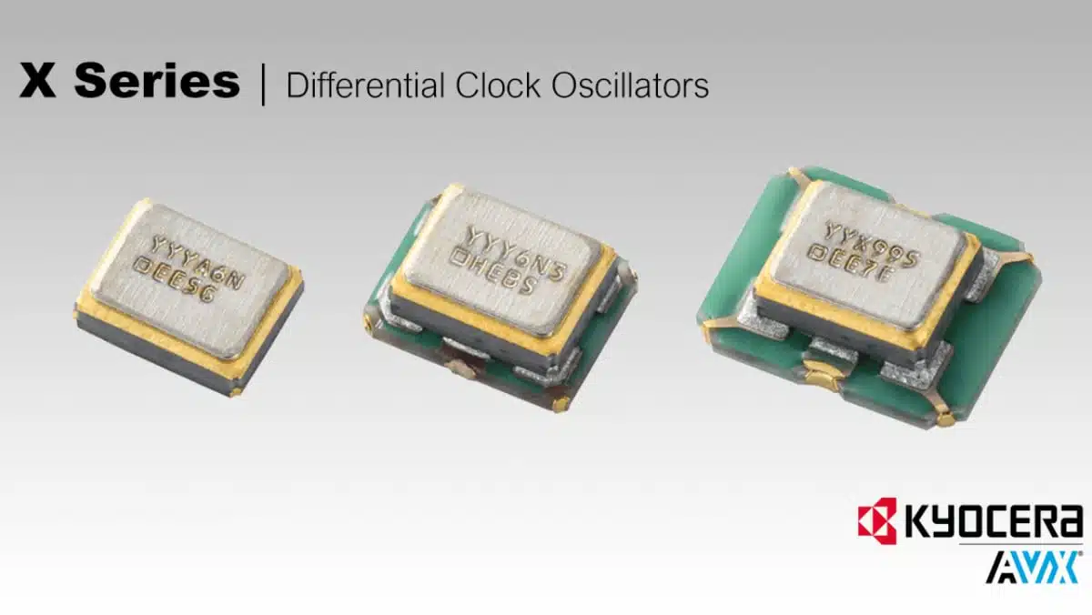
Kyocera’s new X Series differential clock crystal oscillators target high‑speed, high‑capacity data communication in AI servers, optical links, storage, and automotive systems.
They combine industry‑leading 30 femtosecond phase jitter with reduced power consumption, making them attractive for designers facing tight jitter budgets and power constraints in dense, high‑speed platforms.
Key features and benefits
The X Series devices are differential clock crystal oscillators optimized for modern high‑speed serial interfaces, where timing noise directly impacts bit error rates and link margin.
Key features include:
- Industry‑leading typical phase jitter down to 30 fs at 312.5 MHz, enabling tighter timing budgets and improved high‑speed link robustness according to the manufacturer.
- Differential LV‑PECL and LVDS outputs for improved common‑mode noise rejection versus single‑ended clocks, supporting long interconnects and high data rates.
- Wide supply voltage options of 1.8 V, 2.5 V, and 3.3 V (with 1.8 V available for LVDS output only), easing integration into mixed‑voltage digital and SerDes rails.
- Compact SMD packages down to 2.0 × 1.6 × 0.5 mm, supporting high‑density layouts in AI accelerator boards and optical modules.
- Extended operating temperature options up to 105°C, supporting demanding server, communications, and automotive environments.
- Tight frequency tolerance and stability (ppm‑class over temperature, supply, and load) according to the manufacturer datasheet, contributing to stable reference clocks over system lifetime.
- Manufacturing at Kyocera’s Higashine plant in Japan, which may be relevant for supply chain and automotive qualification strategies.
Practical benefits for designers:
- Lower phase jitter helps preserve eye opening in multi‑gigabit links, particularly in systems that already push channel loss and equalization limits.
- Lower current consumption directly eases thermal design and power‑budget allocation in dense AI servers and line cards.
- Small footprints and multiple package options give PCB designers flexibility when routing around large BGAs, power stages, or high‑speed connector regions.
- Extended temperature range and controlled aging characteristics support long‑term stability in infrastructure and automotive use cases.
Typical applications
The X Series is explicitly positioned for high‑speed, large‑capacity data communication systems where low jitter and differential signaling are mandatory rather than optional.
Highlighted application areas:
- AI servers and accelerator platforms, providing low‑jitter references for high‑speed SerDes, PCIe, CXL, and high‑bandwidth memory interfaces.
- Optical transceivers, including 100G/200G/400G+ pluggable modules and line‑cards, where reference clock jitter directly affects optical modulation performance.
- Storage systems, such as enterprise SSDs and storage controllers, requiring clean reference clocks for high‑speed serial interfaces.
- Automotive ADAS equipment, including sensor fusion ECUs, domain controllers, and high‑speed in‑vehicle networks requiring low‑noise, high‑reliability clock sources.
Beyond the listed examples, similar requirements appear in:
- 5G base stations and fronthaul/backhaul equipment with stringent timing and synchronization requirements.
- High‑end test and measurement equipment, routers, switches, and industrial edge servers using high‑speed serial backplanes.
Technical highlights
The X Series combines a high‑quality crystal with advanced oscillator ICs and Kyocera’s proprietary manufacturing technologies to achieve its jitter and power targets.
Package sizes
Available maximum package sizes:
- 2.0 × 1.6 × 0.5 mm
- 2.5 × 2.0 × 0.5 mm
- 3.2 × 2.5 × 0.5 mm
These package options allow trade‑offs between ease of routing, manufacturability, and board space. The smallest 2.0 × 1.6 mm variant is suitable for dense optical modules or compact AI accelerator boards, while larger packages may ease PCB design in lower‑density systems.
Output frequencies and types
Nominal output frequency options:
- 100 MHz
- 125 MHz
- 156.25 MHz
- 312.5 MHz
Output types:
- LV‑PECL
- LVDS
These frequencies align with common reference values for Ethernet, PCIe, and related high‑speed serial standards. For example, 156.25 MHz is widely used in 10G/40G/100G Ethernet and related SerDes clocks, while 312.5 MHz can be used in higher data‑rate or multiplied‑clock architectures. LV‑PECL is often chosen where maximum performance and signal swing are desired, while LVDS supports lower power and simpler termination in many designs.
Phase jitter and current consumption
Typical jitter performance:
- 40 fs at 156.25 MHz
- 30 fs at 312.5 MHz
Typical current consumption (selected cases):
- 29 mA (LV‑PECL output) at 156.25 MHz
- 14 mA (LVDS output) at 156.25 MHz
- 45 mA (LV‑PECL output) at 312.5 MHz
- 23 mA (LVDS output) at 312.5 MHz
According to Kyocera, the 29 mA LV‑PECL 156.25 MHz configuration represents approximately a 42% reduction in current versus a typical 50 mA of conventional solutions at similar conditions. For system designers, this translates into a meaningful reduction in clock tree power consumption, particularly when multiple such oscillators populate large boards.
In practice, lower phase jitter improves timing margin at the receiver and helps reduce bit error rate, especially when other parts of the channel (connectors, vias, cables) already contribute significant noise and distortion. System‑level timing budgets often express total jitter as a root‑sum‑square of multiple contributions, so reducing the oscillator contribution from, for example, tens of femtoseconds to around 30 fs can free margin for other elements.
Supply voltage and temperature ratings
Supply voltages:
- 1.8 V
- 2.5 V
- 3.3 V
(1.8 V is available for LVDS output only, according to the manufacturer.)
Operating temperature ranges:
- –40 to +85°C
- –40 to +105°C
These ranges support both traditional commercial/industrial temperature applications and extended‑temperature systems such as telecom infrastructure and automotive. The tighter frequency tolerance and stability are specified in terms of:
- Initial frequency tolerance at 25°C.
- Frequency stability over operating temperature range.
- Frequency stability versus power supply variations.
- Frequency stability versus load capacitance variations.
- Frequency aging (first year at 25°C).
- Resistance to vibration and shock.
Exact ppm values and test conditions should be taken from the official datasheet for detailed timing budgets and worst‑case analysis.
Availability and production plan
Mass production of the X Series differential clock crystal oscillators began in January 2026 with an initial capacity of approximately 200,000 units per month. Kyocera plans to ramp production to around 2 million units per month from June, responding to growing demand driven by generative AI and the expansion of the AI server market.
For purchasing teams, this ramp suggests:
- A roadmap toward higher volume availability suited to large AI and cloud deployments.
- A defined production base at the Higashine Plant in Yamagata, Japan, which may be relevant for vendor qualification, origin requirements, and risk assessments.
- The expectation that distributor stock and sampling options should improve as the ramp progresses.
Specific ordering part numbers, screening options, and automotive‑grade variants (if available) should be sourced from Kyocera’s product pages and component search tools, as the press release does not provide full ordering code breakdowns.
Design‑in notes for engineers
When designing in the X Series oscillators, engineers should consider both the electrical performance and layout implications in high‑speed systems.
Key design‑in considerations:
- Jitter budget: Incorporate the specified 30–40 fs typical jitter into a complete jitter budget for the target interface, including PLLs, SerDes, connectors, and PCB traces. Check worst‑case values in the datasheet, not only typical figures.
- Output format selection: Choose LV‑PECL where maximum signal integrity margin and higher amplitude are required; choose LVDS when lower power and simpler termination are preferred. Verify the receiver input requirements (common‑mode, swing, termination) against the clock output.
- Supply voltage domain: Align the chosen oscillator supply (1.8 V, 2.5 V, or 3.3 V) with the system’s clocking and SerDes power domains to minimize level shifting and reduce noise coupling.
- Layout and routing: Place the oscillator as close as practical to the device it clocks, route the differential pair with controlled impedance and tight pair coupling, avoid unnecessary stubs, and keep aggressor signals away to preserve jitter performance.
- Decoupling and grounding: Use local decoupling capacitors and a low‑impedance ground return to minimize supply noise, as power‑supply fluctuations can translate into additional phase noise and jitter.
- Thermal considerations: Even with reduced current consumption, in dense AI or telecom cards the cumulative heat from many oscillators and high‑speed devices can be significant. Confirm junction temperature estimates under worst‑case ambient and airflow conditions.
- Reliability and environment: For automotive and harsh‑environment applications, confirm vibration, shock, and long‑term aging specifications against system requirements. Frequency stability and aging data are especially important in long‑life systems.
Purchasing and engineering teams should coordinate early to verify lead times, preferred packages, and any special screening or qualification requirements, particularly for automotive and extended‑temperature designs.
Source
This article is based on information provided by Kyocera Corporation in its official press release about the X Series differential clock crystal oscillators, supplemented by high‑level engineering context and selection considerations for design and procurement teams. For exact ratings, tolerances, and detailed ordering information, always refer to the official manufacturer datasheet and product pages.