Passive Components Blog
No Result
View All Result
  • Home
  • NewsFilter
    • All
    • Aerospace & Defence
    • Antenna
    • Applications
    • Automotive
    • Capacitors
    • Circuit Protection Devices
    • electro-mechanical news
    • Filters
    • Fuses
    • Inductors
    • Industrial
    • Integrated Passives
    • inter-connect news
    • Market & Supply Chain
    • Market Insights
    • Medical
    • Modelling and Simulation
    • New Materials & Supply
    • New Technologies
    • Non-linear Passives
    • Oscillators
    • Passive Sensors News
    • Resistors
    • RF & Microwave
    • Telecommunication
    • Weekly Digest

    Würth Elektronik Expands its MagI³C-VDMM MicroModules

    Guerrilla RF Sponsors Modelithics Models for GaN Power Transistor Line

    Exxelia Presents Smart Integrated Magnetics Solution at Space Tech Expo 2025 

    Littelfuse Releases Load-Powered Compact Relay

    Murata Expands High Cutoff Frequency Chip Common Mode Chokes

    Transformer Design Optimization for Power Electronics Applications

    Microhardness — the Hidden Key to Understanding MnOx Cathode Quality in Tantalum Capacitors

    Samsung to Invest in its Philippine MLCC Facility to Meet Automotive Demand

    Lightweight Model for MLCC Appearance Defect Detection

    Trending Tags

    • Ripple Current
    • RF
    • Leakage Current
    • Tantalum vs Ceramic
    • Snubber
    • Low ESR
    • Feedthrough
    • Derating
    • Dielectric Constant
    • New Products
    • Market Reports
  • VideoFilter
    • All
    • Antenna videos
    • Capacitor videos
    • Circuit Protection Video
    • Filter videos
    • Fuse videos
    • Inductor videos
    • Inter-Connect Video
    • Non-linear passives videos
    • Oscillator videos
    • Passive sensors videos
    • Resistor videos

    Transformer Design Optimization for Power Electronics Applications

    Common Mode Chokes Selection for RF Circuits in Next-Generation Communication Systems

    Capacitor Self-balancing in a Flying-Capacitor Buck Converter

    How to Select Ferrite Bead for Filtering in Buck Boost Converter

    Power Inductors Future: Minimal Losses and Compact Designs

    Percolation Phenomenon: Degradation of Molded Power Inductors in DC/DC Converters

    Connector PCB Design Challenges

    Efficient Power Converters: Duty Cycle vs Conduction Losses

    Ripple Steering in Coupled Inductors: SEPIC Case

    Trending Tags

    • Capacitors explained
    • Inductors explained
    • Resistors explained
    • Filters explained
    • Application Video Guidelines
    • EMC
    • New Products
    • Ripple Current
    • Simulation
    • Tantalum vs Ceramic
  • Knowledge Blog
  • Suppliers
    • Who is Who
  • PCNS
    • PCNS 2025
    • PCNS 2023
    • PCNS 2021
    • PCNS 2019
    • PCNS 2017
  • Events
No Result
View All Result
Passive Components Blog
No Result
View All Result

iPhone X fight for space using A11 chip with embedded passives

8.11.2017
Reading Time: 3 mins read
A A

source: macrumours article

As the launch of Apple’s iPhone X happened in November 17, eager users are set to enjoy battery life normally reserved for Apple’s Plus-size form factors in a phone more closely resembling a non-Plus variant in its dimensions. The reason for this advancement is not an energy density development, but rather a smaller printed circuit board (PCB) inside the iPhone X, according to a February report from KGI Securities.

RelatedPosts

Würth Elektronik Expands its MagI³C-VDMM MicroModules

Guerrilla RF Sponsors Modelithics Models for GaN Power Transistor Line

Exxelia Presents Smart Integrated Magnetics Solution at Space Tech Expo 2025 

This smaller PCB is thanks to a technology referred to as substrate-like PCBs, or SLP. Depictions from the report show a PCB with more layers than a traditional iPhone PCB thanks to application processor and RF signal-chain dedicated PCBs married via an interposer, creating a layer stackup nearly twice that of a conventional iPhone PCB.

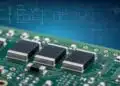
However, this doesn’t come close to telling the whole story. While a new PCB stackup may offer some more flexibility in component placement, it’s important to remember that the opposite side of the board from the A11 isn’t empty in an iPhone 8. There are plenty of components there too — the NFC chip, display drivers, Wi-Fi combo chips, and power management ICs have all often found their homes directly opposite the workhorse application processor.

After all, 4.7-inch iPhones and their 5.5-inch “Plus” siblings have similarly sized PCBs, with battery capacity suffering as a direct result in the smaller phones. Herein lies the real problem in trying to improve battery life in these smaller form factors.

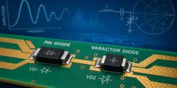
To truly make advances in the space needed to house all the components in the iPhone, the height of the PCBs must be leveraged as well. 3D and 2.5D IC techniques such as chip stacking, through-silicon vias, interposers and other techniques have gotten a lot of exposure in recent years for device packaging, but they can also apply to PCBs to some extent. PCB vendors have been embedding simple passive components such as resistors, capacitors, and inductors in PCBs for years.

These features were first intrinsic to the process, whether through resistor films, printed winding traces, or using the PCB dielectric as the foundation for a capacitor formed across layers. Embedded physical components are now rising in prominence, with vendors even planning for embedded active components in the not too distant future.

Embedded and formed wafer level components

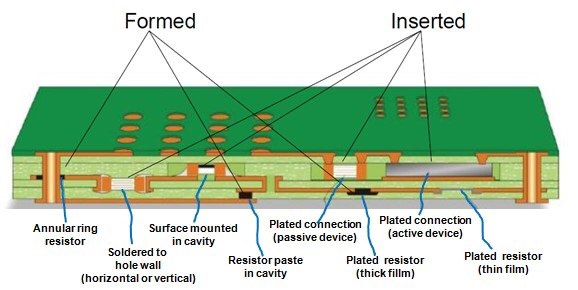
Though it has gone somewhat unnoticed, Apple has already been employing this technique with its A-series application processors. Several years ago, leaked packaged parts began to show curious voids on the underside where the normal interconnect array would be expected. These voids are likely spaces for passive filtering components to nestle inside the package.

Apple A11 chip with embedded components

This achieves two things. First, it decreases the amount of board space needed to seat all components. Second, it often carries a performance advantage because proximity to the metal inside the device is one of the key performance drivers of active devices such as this.

The capacitors and inductors used to filter and bypass the power on the application processor serve to prevent voltage droop in changing current demand scenarios, as well as provide a bypass route to ground for high frequency noise. Placing it as close to the device as possible cuts down on unwanted parasitics which reduce these components’ effectiveness.

Passive filtering components for the A11 on an iPhone 8 Plus PCB

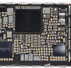
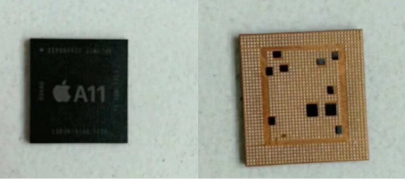
By extending this concept to PCBs, Apple can utilize any extra space within the PCB to house these components. Examination of the rear of an iPhone 8 Plus PCB shows there are numerous passive components sitting on the rear of the PCB behind the A11.

The more of these components that can be embedded within the board stackup, the more space efficiency the design can have. At an extreme, the PCB would have these components untouched, with an interposer (or perhaps multiple, interspersed with bonding material to match the boards) having a cutout in this area so that the digital and RF boards could be laminated together. This concept in itself presents technical challenges, and a gradual adoption rather than a momentous shift should be expected for embedded components.

What should be clear moving forward is that the internals of PCB stackups could prove to be just as interesting as their surfaces and the x-ray shots of component dies that we have come to expect. Perhaps we’ll get a glimpse at some of these concepts once the teardowns start rolling in.

Related

Recent Posts

Exxelia Presents Smart Integrated Magnetics Solution at Space Tech Expo 2025 

5.11.2025
8

Murata Expands High Cutoff Frequency Chip Common Mode Chokes

5.11.2025
4

Transformer Design Optimization for Power Electronics Applications

4.11.2025
7

Microhardness — the Hidden Key to Understanding MnOx Cathode Quality in Tantalum Capacitors

3.11.2025
15

Samsung to Invest in its Philippine MLCC Facility to Meet Automotive Demand

3.11.2025
15

Lightweight Model for MLCC Appearance Defect Detection

3.11.2025
15

DMASS Reports First Positive Signs of European Distribution Market in Q3/25

3.11.2025
7

TAIYO YUDEN Releases 22uF MLCC in 0402 Size for AI Servers

3.11.2025
8

Bourns Releases High Current Metal Alloy-based, Multilayer Power Chip Inductors

31.10.2025
25

Bourns Unveils High-Precision Wirewound Resistor with Long-Term Stability

30.10.2025
23

Upcoming Events

Nov 4
November 4 @ 12:00 - November 6 @ 14:15 EST

Wirebond Materials, Processes, Reliability and Testing

Nov 6
14:30 - 16:00 CET

Self-healing polymer materials for the next generation of high-temperature power capacitors

Nov 11
17:00 - 18:00 CET

Industrial Applications Demand More from Interconnects in Next-Gen Designs

View Calendar

Popular Posts

  • Buck Converter Design and Calculation

    0 shares
    Share 0 Tweet 0
  • Boost Converter Design and Calculation

    0 shares
    Share 0 Tweet 0
  • LLC Resonant Converter Design and Calculation

    0 shares
    Share 0 Tweet 0
  • Flyback Converter Design and Calculation

    0 shares
    Share 0 Tweet 0
  • Ripple Current and its Effects on the Performance of Capacitors

    3 shares
    Share 3 Tweet 0
  • MLCC and Ceramic Capacitors

    0 shares
    Share 0 Tweet 0
  • Dual Active Bridge (DAB) Topology

    0 shares
    Share 0 Tweet 0
  • What is a Dielectric Constant and DF of Plastic Materials?

    4 shares
    Share 4 Tweet 0
  • SEPIC Converter Design and Calculation

    0 shares
    Share 0 Tweet 0
  • Flying Capacitors

    0 shares
    Share 0 Tweet 0

Newsletter Subscription


Passive Components Blog

© EPCI - Leading Passive Components Educational and Information Site

  • Home
  • Privacy Policy
  • EPCI Membership & Advertisement
  • About

No Result
View All Result
  • Home
  • Knowledge Blog
  • PCNS

© EPCI - Leading Passive Components Educational and Information Site

This website uses cookies. By continuing to use this website you are giving consent to cookies being used. Visit our Privacy and Cookie Policy.
Go to mobile version