


This article elaborates on design and calculation of SEPIC DC/DC converters. The post is based on Würth Elektronik‘s “DC/DC Converter Handbook” that can be ordered from WE website here. Published under permission from Würth Elektronik.
Key Takeaways
- The article details the design and calculation of SEPIC DC/DC converters, highlighting their advantages and limitations.
- SEPIC converters handle varying input and output voltages efficiently without drawing discontinuous currents.
- Key considerations include component selection: use low ESR capacitors and appropriate inductors for better performance.
- The SEPIC converter design should minimize interference using careful layout and filtering techniques.
- Practical calculations for component values include inductor and capacitor sizing based on voltage ripple and current requirements.
SEPIC Converter Block Diagram and General Thoughts
If the input voltage (e.g., lithium-ion battery) is larger or smaller than the output voltage during operation, then the SEPIC (Single Ended Primary Inductance Converter) topology is a possible choice. You can see overview of power converters in article DC-DC Converter Basic Characteristics and Formulas.
This has the advantage of being inherently short-circuit proof thanks to the coupling capacitor in series with the MOSFET. A SEPIC converter can also be built with many common boost controller ICs, which offers advantages in terms of availability and cost. Another advantage of the SEPIC controller is that it does not draw discontinuous currents at the input and so does not unnecessarily load a battery.
Limitations do arise however with high output currents. As the most common SEPIC converters are built with Schottky diodes for commutation, this topology has lower efficiency at higher currents. Another critical component is the coupling capacitor. A very high AC current flows through this component from input to output. A capacitor with a very low ESR must therefore be used here; a parallel connection of several capacitors is also suitable for reducing the total ESR. MLCCs ceramic capacitors with X7R ceramic are ideally suited for this purpose.
Above 50 W, the fully synchronous buck-boost topologies are then usually beneficial due to the low RDS, on losses of the FETs used. However, with the fully synchronous buck-boost converters, the semiconductor cost ratio is relatively high, so that up to 50 W the SEPIC is often advantageous from a cost perspective.
This power-range guidance lines up with our cross-topology mapping of dominant passives for non-isolated converters:
| Topology | Isolation | Typical Power Range | Dominant Passive Components | Primary Passive Concerns |
|---|---|---|---|---|
| SEPIC | No | <50 W | Coupling capacitor, coupled inductors, C~out~ | Coupling capacitor AC stress; core loss and leakage |
Source: Passive Components for Power Converters Dossier, Passive Components Blog.
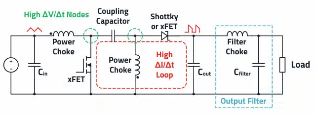
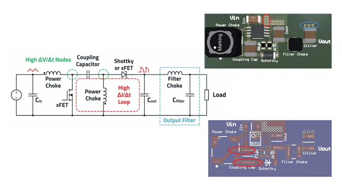
The SEPIC converter, as apparent from Figure 1., also has a critical current loop with a high ΔI/Δt at the output, which is a source of differential-mode interference. Unlike the boost converter, there are two “hot nodes” with high ΔV/Δt. The hot nodes are mainly the source of common-mode interference.
From the EMC perspective, the SEPIC converter is therefore similar to a boost converter in many respects. An output filter must often be connected downstream to attenuate both the high frequency interference and the slightly lower-frequency voltage ripple.
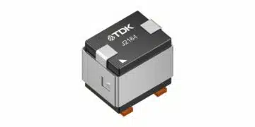
Storage inductors with two galvanically isolated windings on the same core are ideal for SEPIC converters. This reduces the current ripple through the individual windings and therefore the minimum inductance values required can also be lower. This, in turn, saves both package space and costs.
In the layout, as in the topologies shown so far, attention must be paid to a “single point power ground concept”. This keeps the current loops (H-field antennas), as well as the parasitic inductance – the cause of differential-mode interference – as small as possible. The area of the two “hot nodes” should also be minimized to keep capacitive couplings small with respect to reference ground, the coupling path for common-mode interference.
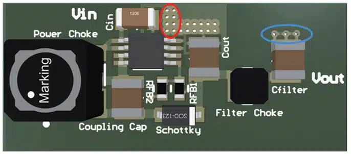
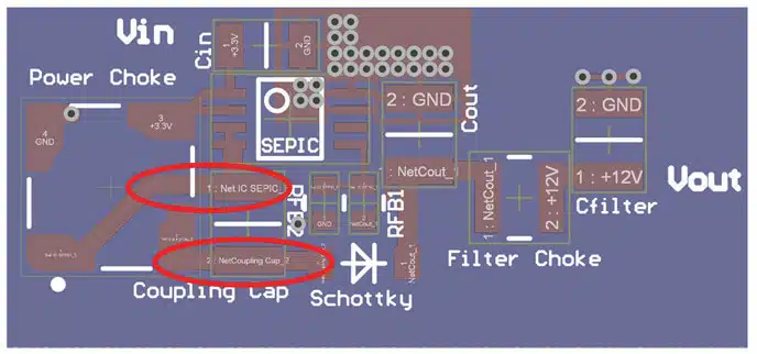
As with the previous topologies, the GND of the optional filter capacitor should be slightly fur ther away at the output to obtain the quietest possible filter GND reference. To keep undesirable output voltage fluctuations low, the feedback resistor network should also be placed close to the regulator. The possibly very long feedback conductor track therefore has a lower impedance and is less sensitive to interference. The output voltage for regulation should
be tapped at a point as close to the output capacitor as possible.
Example SEPCI Converter Design and Calculation
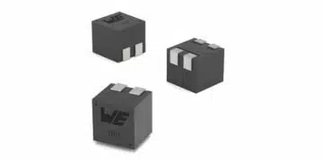
storage inductor (double) for a sepic converter
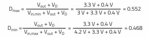
Input voltage: Vin = 3 to 4.2 V (voltage range, e.g. Li-Ion battery)
Output voltage: Vout = 3.3 V
Output current: Iout = 1 A max.
Switching frequency: fsw = 500 kHz
Max. bandwidth control loop/crossover frequency: fc = 10 kHz
Forward voltage rectifier diode: VD = 0.4 V
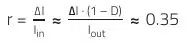
Ripple current factor:
Duty cycle D:
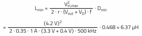
The minimum required inductance results at maximum input voltage (4.2 V) and the resulting minimum duty cycle:
The ripple current factor refers to the “top” winding of the double choke, which consequently has the input current flowing through it.
Considering a standard inductance value of a double choke with 6.8 µH, this results in a maximum ripple current of:
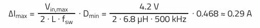
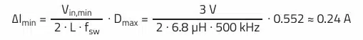
Although the ripple current also reaches its maximum at the maximum input voltage, the minimum ripple current at the minimum input voltage must be taken for the subsequent calculation of the maximum peak inductor current and the RMS current for the output capacitor. This is due to the fact that the effect of ripple current decrease at low input voltage is completely compensated by the simultaneous increase of input current for standard ripple current factors of 0.3…0.6.
Rated Current Ir:
Often it is sufficient to select the rated current based on the average inductor current with some margin. In fact, the RMS value of the inductor current (average inductor current + AC ripple current) is responsible for the heat generated by the DC resistance (see RMS chapter in Selection of Storage Inductors for DC/DC Converters).
The SEPIC has the special feature that the input current flows in one winding and the output current flows in the other winding as the average inductor current. The rated current of a double choke is specified for each winding and is the same for both windings with a 1:1 transformation ratio. You are therefore always on the safe side if the rated current is selected with some margin, greater than the maximum input current in boost mode. The maximum input current is estimated here using the output power and the diode conduction losses. As this simplification results in additional errors (e.g., the influence of switching losses on the input current is neglected), the rated current margin for the SEPIC should be larger than for the buck.
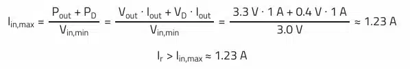
A choke with more than 1.23 A rated current (according to datasheet) should be selected.
Saturation Current Isat:
Half the AC ripple current must be added to the average inductor current to determine the maximum peak current. The average inductor current of the top winding corresponds to the input current in the SEPIC. As for the rated current, the saturation current of a double choke is specified for each winding. You are therefore on the safe side here if the saturation current is selected with some margin, greater than the maximum peak inductor current.
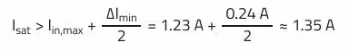
The double windings in question should therefore have an inductance of 6.8 µH per winding, a rated current of approximately 1.5 A and a saturation current of minimum 1.7 A. This means that in most applications there is sufficient margin regarding component tolerances and temperature dependence. A double choke, such as the WE-DD shielded coupled inductor, meets these requirements.
The fastest and easiest way to get there is to use the REDEXPERT inductor simulation tool.
Input capacitor for a SEPIC converter
RMS current (ripple current) through the input capacitor:
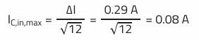
With the help of the REDEXPERT tool, a capacitor can now be selected with the lowest possible impedance at the switching frequency of 500 kHz which, at the same time, meets the requirements in terms of the ripple current as well as voltage.
Output Capacitor for a SEPIC Converter
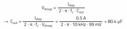
The output capacitor is defined based on the maximum permissible voltage ripple and on the basis of the maximum permissible voltage change (Vdroop) resulting from a load step. In our example we want to achieve a maximum voltage ripple of 1% (33 mV) at an output voltage of 3.3 V. The maximum voltage change should be 3% (99 mV) for a load step from 0.5 A to 1 A (Istep = 0.5 A).
From these assumptions, the minimum necessary capacitance can be calculated, which fulfills both requirements. For the output voltage residual ripple, in addition to the capacitance-dependent part, the influence of the ESR is considered (the ESL is neglected). For simplicity, an even split is assumed for the two components, resulting in 16.5 mV each for the capacitance and the ESR calculations. With the SEPIC converter, the extent to which this addition actually occurs, depends on the duty cycle and the magnitude of the ripple current.
In addition, it must be checked mathematically whether the AC current through the output capacitor stays below the maximum ripple current according to the datasheet.
The next equation describes the relationship between the output capacitance and the ripple voltage for a SEPIC converter topology (assumption: ideal capacitor):
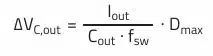
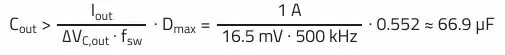
This equation is used to calculate the minimum capacitance required for the given capacitance dependent ripple:
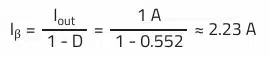
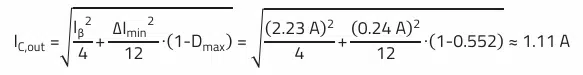
For the SEPIC converter topology, the additional calculation is needed to calculate the average current amplitude of the output capacitor current:
The equation describes the relationship between the ESR of the output capacitor and the ripple voltage for a SEPIC converter topology (assumption: ESL is neglected):
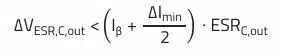
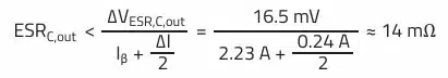
The next equation is used to calculate the maximum allowable ESR of the output capacitor based on the given ESR-dependent ripple voltage:
This equation is used to calculate the minimum output capacitance to maintain a given voltage droop during a load step:
The following equation is used to determine the RMS current that flows through the output capacitor of the SEPIC converter:
The capacitance of 66.9 µF is not relevant in this case, as the minimum necessary capacitance of 80.4 µF results from the maximum allowed voltage change during load transients. Based on the results, we therefore need a capacitor with a capacitance of least 82…100 µF (default value) and an ESR lower than 41.7 mΩ at 500 kHz.
A low ESR H-chip aluminum polymer SMT capacitor, such as the WCAP-PHLE (875035019001), is a suitable choice for this purpose. This offers a stable capacitance of 100 µF in a very small package (7.3 · 4.3 · 1.9 mm³), a 4 mΩ ESR at 500 kHz and is specified for a maximum ripple current of up to 6.3 A.
Design of the input and output filters for a SEPIC converter
Design is carried out according to the same principle as previously explained in chapter as explained in the Example Buck Converter Design and Calculation.
Read also the related articles in this series:
For how the SEPIC’s coupling-capacitor stress and power range compare with buck, boost and tapped-inductor buck topologies, see our Passive Components for Power Converters Dossier.
- Selection of Capacitors for DC/DC Converters
- Selection of Storage Inductors for DC/DC Converters
- Input filters for DC/DC converters
- Switching vs Linear Power Converters Compared
- Buck Converter Design and Calculation
- Boost Converter Design and Calculation
- Flyback Converter Design and Calculation
- Fly-Buck Converter Explained and Comparison to Flyback
- LLC Resonant Converter Design and Calculation
SEPIC and Flyback Converter Basic Formulas
The following table 1. provides basic formulas of the SEPIC and flyback converter topologies.
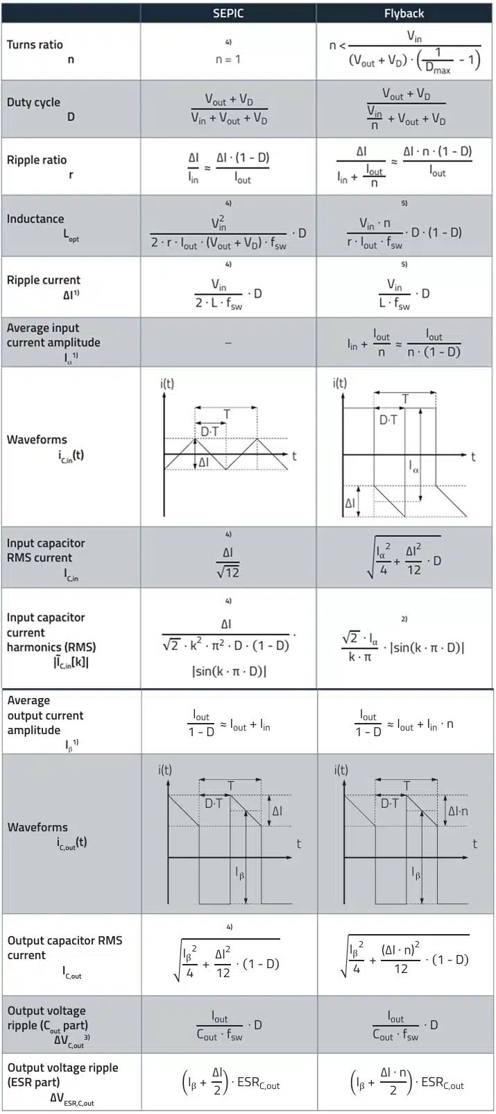
1) These assumptions apply to the ideal switching regulator in continuous conduction mode
(CCM), i.e., the efficiency of the converter is assumed to be 100% (η = 1).
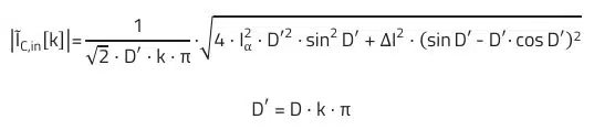
2) The current curve from this equation is approximately rectangular (ΔI neglected). Exactly:
3) The equations defined for ΔVC,out apply to the ideal capacitor. Cout therefore defines the minimum capacitance to meet the ripple voltage requirement. The actual voltage ripple will be higher due to the parasitic inductance ESL (equivalent series inductance) and ESR (equivalent series resistance) of the capacitor.
4) These equations only apply for a coupled choke with a turns ratio of 1:1 (n=1).
5) L corresponds to the main inductance (primary inductance) of the transformer.
Frequently Asked Questions about SEPIC Converter Design
A SEPIC (Single-Ended Primary Inductor Converter) is a DC/DC converter topology that can step up or step down voltage, making it suitable when input voltage may be higher or lower than the desired output. It is inherently short-circuit proof due to its coupling capacitor.
SEPIC converters offer continuous input current, compatibility with common boost controller ICs, and cost efficiency up to about 50 W. They also minimize battery stress compared to discontinuous input topologies.
Efficiency decreases at higher output currents due to Schottky diode losses. The coupling capacitor must handle high AC currents and requires very low ESR, often achieved with parallel MLCCs. Above 50 W, synchronous buck-boost topologies are usually more efficient.
Key components include the coupled inductor (double choke), low-ESR input and output capacitors, and a suitable rectifier diode. Layout considerations, such as minimizing hot node areas and ensuring single-point grounding, are also essential.
SEPIC converters are ideal for applications where the input voltage fluctuates above and below the output voltage, such as battery-powered devices. They are cost-effective up to 50 W and provide stable operation with proper filtering.
How to Design a SEPIC Converter
- Define Input and Output Requirements
Specify input voltage range (e.g., 3–4.2 V from a Li-Ion battery), desired output voltage (e.g., 3.3 V), maximum output current (e.g., 1 A), and switching frequency (e.g., 500 kHz).
- Select the Inductor
Choose a coupled inductor (double choke) with sufficient inductance (e.g., 6.8 µH per winding), rated current above the maximum input current, and saturation current above the peak inductor current.
- Choose the Input Capacitor
Calculate RMS ripple current and select a capacitor with low impedance at the switching frequency. Use simulation tools like REDEXPERT to optimize selection.
- Choose the Output Capacitor
Determine capacitance based on maximum ripple voltage (e.g., 1% of Vout) and transient response requirements. Ensure ESR is low enough to meet ripple specifications (e.g., < 41.7 mΩ at 500 kHz).
- Optimize Layout
Minimize hot node areas, use a single-point ground concept, and place feedback resistors close to the regulator. Add an output filter if necessary to reduce EMI and ripple.
- Validate with Simulation and Testing
Use tools like REDEXPERT to simulate performance, then verify with real measurements to ensure stability, efficiency, and compliance with EMI requirements.